Skip to content
In 2024, the global semiconductor industry did not experience the expected full recovery, but the rapid development of generative artificial intelligence (AIGC), automotive electronics, and communication technology has laid the foundation for underlying technologies in 2025, bringing new hope for the semiconductor industry to warm up in the new year.
This year, we witnessed the widespread application of silicon carbide (SiC) power devices in electric vehicles, innovative applications of chiplet technology in high-performance AI chip design, and the rapid rise of RISC-V architecture in automotive electronics and other fields. Additionally, fourth-generation semiconductor materials—such as gallium oxide (Ga2O3) and aluminum nitride (AlN)—have also begun to emerge, showcasing enormous potential.
In terms of the market, despite numerous challenges facing the global economy, the semiconductor industry has maintained strong growth momentum. According to the World Semiconductor Trade Statistics Organization, the global semiconductor market size is expected to reach $611.2 billion in 2024, a year-on-year increase of 7%. Particularly in automotive electronics, industrial automation, and consumer electronics, market demand remains robust, driving rapid development across the entire industry.
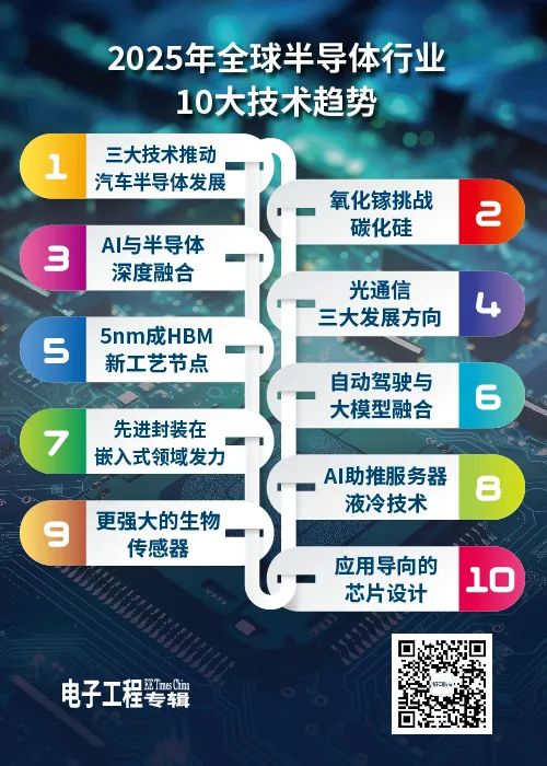
Looking ahead to 2025, the global semiconductor market is expected to grow by 12.5%, reaching a valuation of $687 billion. Based on discussions with industry experts and manufacturers throughout the year, Electronic Engineering Times has summarized and analyzed the ten major technology trends expected to emerge or develop rapidly in the global semiconductor industry in 2025. This article will explore the development direction and market prospects of these advanced technologies.
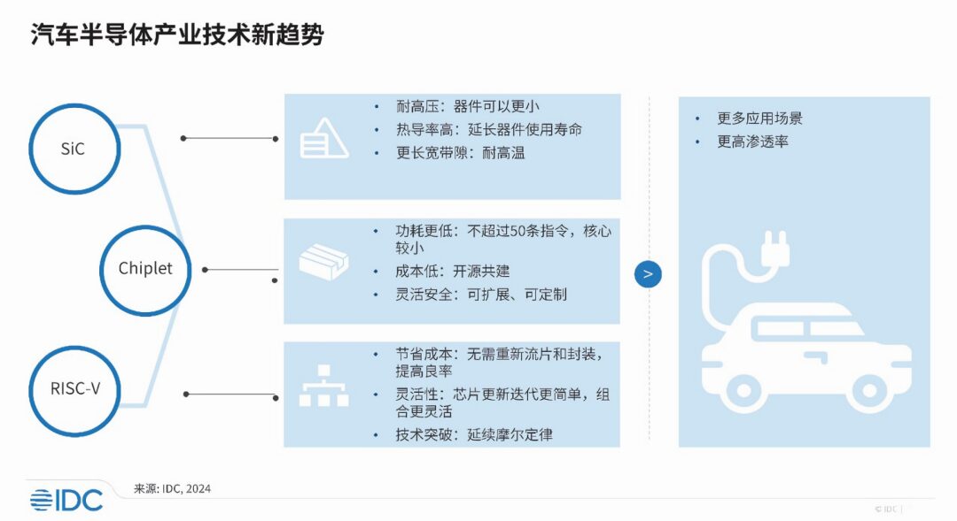
SiC, Chiplet, and RISC-V Join Forces to Promote Automotive Semiconductor Development
Chips, as the high ground in the race for automotive intelligence, have become the key core of global smart car competition. In 2025, SiC, Chiplet, and RISC-V are expected to continue collaborating to promote the development of the automotive semiconductor industry (Figure 1).
Figure 1: The three technologies—SiC, Chiplet, and RISC-V—are expected to continue driving the development of the automotive semiconductor industry. (Source: IDC)
“800V+SiC” Will Become Standard for High-End Electric Vehicles
A clear trend observed is that as automotive manufacturers pursue greater energy efficiency and range, vehicle manufacturers will release more models equipped with an 800V platform in the next two to three years, significantly increasing the demand for SiC power devices. It can be said that “800V+SiC” has basically become standard for high-end electric vehicles.
We make some judgments on the future development trends of silicon carbide technology from three aspects. First, from the material perspective, based on the demand for cost and yield, wafer materials are evolving towards large-size, low-defect SiC substrates and epitaxy preparation; from the device perspective, the pursuit is for lower on-resistance of SiC MOSFETs while achieving reliability and robustness levels closer to silicon-based IGBTs; from the process perspective, there is a continued study of the fundamental scientific issues restricting SiC MOSFET development, such as improving channel mobility through the use of high-purity SiC substrates and refining gate oxide layer fabrication processes.
Chiplet Chips Become New Breakthroughs in Automotive High-Performance SoC Development
As a representative of modular chip design technology, Chiplet is an innovative solution that reduces costs and increases efficiency, addressing the demand for high-performance SoC chips in automotive applications. Its functions are independent as Chiplets, and by selecting mature processes and chips, production yield can be improved, and development cycles shortened. However, challenges are also evident. For instance, communication interfaces between different chips from different manufacturers vary; as chip integration increases, power consumption, heat dissipation, and data transmission security face higher requirements.
RISC-V Becomes a New Choice After Arm Architecture
Compared to x86 and Arm, RISC-V has a more streamlined instruction set, free from legacy issues, and operates at very low power. These characteristics make RISC-V particularly suitable for enhancing the overall performance of automotive systems while reducing manufacturing costs. In specific applications, RISC-V processors can be widely used in key areas such as in-vehicle infotainment systems, autonomous driving control systems, battery management systems, and vehicle network communications. In the next 3 to 5 years, the shipment volume of RISC-V architecture chips in the automotive industry is expected to grow at an annual rate of 66%.
Fourth-Generation Semiconductor Materials: Gallium Oxide Will Directly Challenge Silicon Carbide
Fourth-generation semiconductor materials include ultra-wide bandgap semiconductors and ultra-narrow bandgap semiconductors, the former includes gallium oxide, diamond, and aluminum nitride, while the latter includes gallium antimonide and indium antimonide. Among them, gallium oxide has a bandgap width of 4.9 eV, surpassing SiC’s 3.2 eV and GaN’s 3.39 eV; moreover, its conduction characteristics are about 10 times that of SiC, with a theoretical breakdown field strength approximately three times that of SiC, and theoretical losses only 1/3000 of silicon, 1/6 of SiC, and 1/3 of GaN. From a cost perspective, gallium oxide’s final device cost based on the same 6-inch substrate is about 1/5 that of SiC, comparable to silicon-based products.
Academician Hao Yue from the Chinese Academy of Sciences predicted two years ago that gallium oxide devices are expected to become competitive power electronic devices within the next decade, directly competing with SiC devices. Leading gallium oxide company FLOSFIA of Japan estimates that by 2025, the gallium oxide power device market size will start to exceed GaN, reaching $1.542 billion by 2030, accounting for 40% of SiC, and 1.56 times that of GaN.
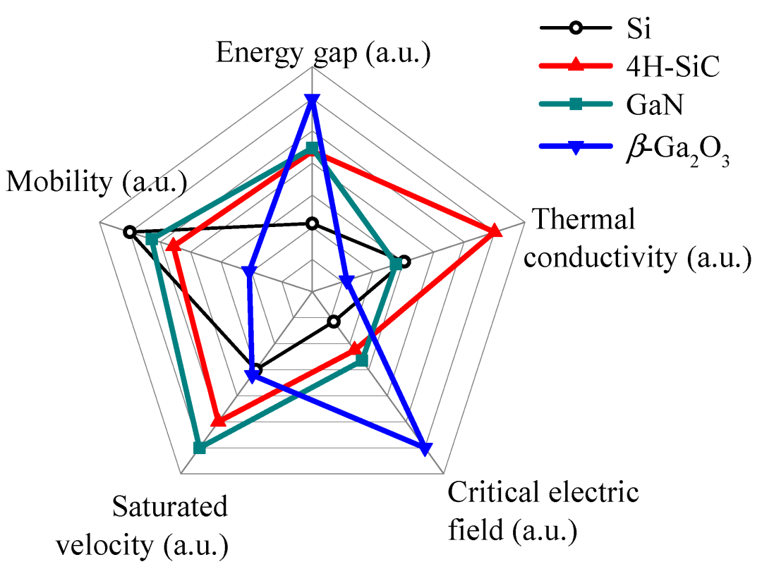
Despite gallium oxide’s significant advantages in cost and performance, its large-size single crystal preparation faces challenges such as high melting points, thermal decomposition, and brittleness. Currently, gallium oxide production in China is limited to laboratories and universities, while Japan is at the forefront of gallium oxide mass production. For example, the FOX company established at Tohoku University in Japan uses non-precious metal single crystal growth technology, aiming to produce low-defect β-Ga2O3 substrates at a lower cost than SiC (Figure 2).
Figure 2: Radar chart of the basic material characteristics of Si, 4H-SiC, GaN, and β-Ga2O3, with all parameters normalized. (Source: MDPI)
Aluminum nitride, as another fourth-generation semiconductor material, is regarded as the preferred material for achieving ultra-low-loss power devices and high-temperature electronic devices due to its large breakdown electric field and low loss characteristics. NTT Corporation successfully produced high-quality aluminum nitride using metal-organic chemical vapor deposition (MOCVD) at the beginning of 2024 and developed methods for forming ohmic and Schottky contacts, demonstrating the operation of aluminum nitride transistors for the first time.
Looking ahead to 2025, as technology advances and mass production challenges are gradually overcome, fourth-generation semiconductor materials such as gallium oxide and aluminum nitride will not only challenge the existing SiC and GaN markets but may also surpass them in specific application areas due to their unique performance advantages.
From Design and Manufacturing to Application: AI and Semiconductors Deeply Integrate
AI is triggering a new round of technological revolution. From language models and multimodal models to single intelligence, to OpenAI’s reasoning using the Chain of Thinking (CoT), and to agents completing complex tasks, AI foundational capabilities are rapidly evolving and quickly integrating into every aspect of production and life, reshaping various industries and triggering a new round of technological and industrial revolution.
Thus, in this technological super cycle, the semiconductor industry has also formed a mutually reinforcing relationship with AI.
For example, in the field of chip design, AI continuously improves design efficiency and accuracy through intelligent algorithms such as machine learning and deep learning, helping designers predict and optimize chip performance and power consumption early in the design phase, reducing design iterations and shortening time-to-market.
In intelligent manufacturing, by adopting AI machine vision automated inspection equipment, not only has the speed of production lines increased, but manufacturing precision has also significantly improved. Meanwhile, by collecting and analyzing production data, AI algorithms can predict equipment failures, reduce unexpected downtime, and optimize manufacturing parameters, minimizing material waste and energy consumption.
With the advancement of various cloud-based AI training and inference application services, global AI server shipments are expected to reach 1.65 million units in 2024, increasing its share to 12.1%. Its overall capital expenditure is expected to grow by about 50%, and it will continue to maintain double-digit growth in 2025. AI servers not only require high-performance hardware support such as GPUs, CPUs, TPUs, and storage, but some leading cloud service providers have even built custom chips specifically for running AI models, which has boosted the semiconductor industry.
At the same time, we must also pay attention to innovations in edge AI technologies such as smartphones, AI PCs, automotive terminals, and industrial IoT, as edge AI has a large market scale, clear business models, and rich application scenarios, making it easier to achieve large-scale AI deployment, thereby accelerating the market demand for high-performance SoCs, NPUs, RF, power management, and analog signal chain components.
While AI brings opportunities to upstream chip design companies, it also provides incremental space for downstream packaging technology. After all, generative AI models require millions or billions of parameters for inference, posing higher demands on chip processing speed, capacity, and bandwidth, which will further drive the development of advanced packaging technologies represented by Chiplet, leading to ecological changes in the packaging industry.
Optical Communication Technology Develops Towards High Capacity, High Speed, and Integration
With the growth of global data traffic, especially in the fields of video streaming, cloud computing, IoT, and 5G networks, the demand for high-speed optical communication solutions is increasing.
In the past year, significant progress has been made in optical communication technology. First, in terms of transmission rates, 400Gbps and even 800Gbps interfaces have become a reality, marking a new milestone in the performance of optical transceivers. Innovations in coherent optical technology and silicon photonics by companies like Huawei and Nokia have been key factors in this achievement, as these new technologies not only enhance data transmission speeds but also reduce power consumption, improving reliability and scalability. Dense Wavelength Division Multiplexing (DWDM) technology further expands the data carrying capacity of a single optical fiber, supporting more users online simultaneously and meeting the growing data demand.
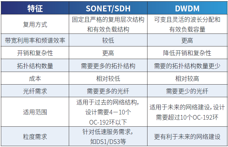
Synchronizing Optical Network (SONET) technology performs excellently in high-bandwidth demand scenarios, especially suitable for financial transaction systems and healthcare, with its high reliability making it an ideal choice for critical applications (Figure 3). Efficient interconnection within and between data centers has also become a research hotspot, driving the development of new optical switches and routers to achieve faster speeds and lower latency data exchanges.
Figure 3: Comparison of SONET/Synchronous Digital Hierarchy (SDH) and DWDM. (Source: QSFPTEK)
Looking ahead to 2025, optical communication technology will continue to develop towards higher capacity, faster transmission rates, lower costs, and broader deployment:
-
Higher Capacity and Faster Transmission Rates: The industry will explore how to utilize advanced modulation formats and technologies to achieve Tbps-level data transmission rates.
-
Edge Computing and Optical Interconnection: Optical interconnection solutions optimized for distributed architectures will become a research focus, providing low-latency, high-bandwidth connectivity to support real-time processing requirements.
-
Integrated and Modular Design: More compact and energy-efficient optical communication modules will be one of the key development directions for the future, helping to reduce operational costs and improve overall energy efficiency.
Despite the bright prospects, high initial deployment costs remain one of the main obstacles to the widespread adoption of optical communication technology. To address this, the industry is seeking solutions through government policy support, technological innovations to reduce costs, and accelerating the standardization process to promote compatibility between different manufacturers’ products, thereby reducing the overall ownership costs for users.
HBM4 Mass Production Timeline Accelerated, 5nm Becomes New Process Node
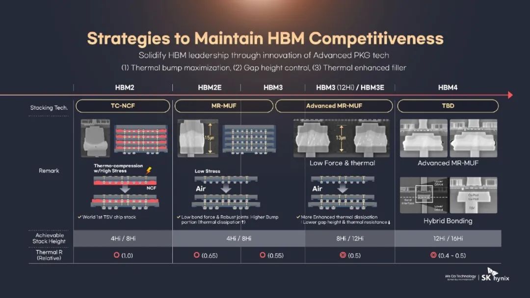
Although HBM4, as the latest generation of high-bandwidth memory technology, has a related mass production schedule in the technology roadmap of major memory chip giants, the demand from AI terminals may force memory manufacturers to accelerate their mass production timelines. In terms of mass production progress, the HBM4 mass production timelines of the three major memory manufacturers—Samsung, SK Hynix, and Micron Technology—are all set for 2025 to 2026.
The biggest application advantage of HBM4 lies in significantly improving memory bandwidth and capacity by increasing the number of stacked layers and channels. However, the HBM4 memory interface has expanded from 1024 bits to 2048 bits, which means that the design and production of HBM4 memory will face new challenges, necessitating the use of more advanced process nodes and more challenging packaging technologies.
From a technological progress perspective, 5nm has become the new process node for HBM4. Meanwhile, chip packaging remains one of the biggest challenges facing HBM4. Since the non-bump hybrid bonding technology is not yet mature, traditional bump-based solutions are expected to remain the mainstream bonding technology for 16-layer stacked HBM4. To ensure that the stack height remains within a certain range, HBM4 needs to further compress the interlayer gap and improve thermal management capabilities. In terms of HBM bonding processes, the three major HBM memory manufacturers are conducting tests and research on processes such as non-solder bonding to promote the mass production of HBM4.
In terms of mass production progress and plans, Samsung Electronics has successfully manufactured 16-layer stacked HBM3 memory based on hybrid bonding technology and plans to apply this technology to HBM4 mass production. Meanwhile, Samsung is establishing a dedicated HBM4 production line, which is currently in the trial production stage, with mass production of 12-layer HBM4 stacks expected in the second half of 2025. SK Hynix is also developing 16-layer stacked HBM4 memory, planning to mass produce it in 2025 (Figure 4). The company is collaborating with TSMC to create the substrate chip for HBM4 packaging using TSMC’s 5nm process. SK Hynix also plans to introduce hybrid bonding technology to reduce the height of storage chip stacking gaps, thereby achieving more stacked layers. Micron Technology’s mass production timeline is slightly later, with plans to launch 12 and 16-layer stacked HBM4 products in 2026.
Figure 4: Development trends of HBM stacking technology. (Source: SK Hynix)
For the technical demands of companies such as SK Hynix, Samsung, and NVIDIA, TSMC will also utilize its N12FFC+ and N5 process technologies, as well as advanced packaging solutions like InFO and CoWoS.
Integrated Central Computing Architecture and Large Models Promote the Development of Autonomous Driving Technology
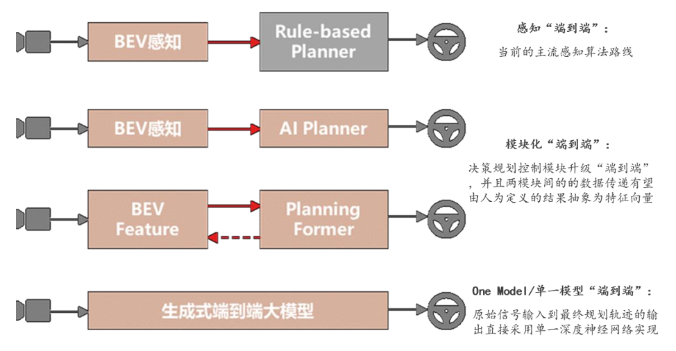
Since the rise of General Artificial Intelligence (AGI), automotive large models have also gained popularity, particularly end-to-end automotive large models, which may become the best route for L2 driving assistance or L3 autonomous driving (Figure 5). The launch of Tesla’s FSD V12 version is a significant marker of this trend, indicating that end-to-end autonomous driving technology has become a reality in mass-produced vehicles. This solution has also been recognized by several automotive manufacturers, with companies like Huawei, Xiaopeng, SenseTime, and Yuanrong Qixing actively following suit in China.
Figure 5: Diagram of the evolution of end-to-end autonomous driving architecture. (Source: Chentao Capital “End-to-End Autonomous Driving Industry Research Report”, Cinda Securities R&D Center)
With the application of large models, the demand for computing power in autonomous driving chips is also continuously increasing, and 2024 is seen as the first year of cross-domain integration. Many companies have released SoC chips that support central computing platforms, such as NVIDIA’s DRIVE Thor and Qualcomm’s Snapdragon Ride Flex SoC, both boasting computing power of up to 2000 TOPS, capable of supporting L4/L5 autonomous driving capabilities while also providing a higher-end smart cabin experience. Many automotive manufacturers and Tier 1 suppliers are actively promoting this direction, and the integration of cabin and driving is expected to become a mainstream trend in the next two years.
The key question is whether the end-to-end large model for intelligent driving can be implemented in vehicles; the development of this technology can be divided into four stages: perception end-to-end, decision planning modeling, modular end-to-end, and One Model end-to-end. The modular end-to-end solution from Chinese autonomous driving companies is expected to be mass-produced and implemented in vehicles by 2025.
From a market perspective, research institutions indicate that the automotive semiconductor market size will reach $100 billion by 2029, with advanced driver assistance systems (ADAS) and safety achieving the highest growth at a compound annual growth rate of 14% from 2023 to 2029. High-performance SoCs, smart cabins, power electronics, and MCUs for future E/E architectures will also be key investment directions for OEMs in automotive semiconductors.
2.5D and 3D Advanced Packaging Continue to Deepen, Showing Potential in Embedded Fields
2.5D packaging technology achieves efficient chip-to-chip communication by integrating multiple chips in an intermediary layer; 3D packaging technology goes further by vertically stacking chips, significantly reducing device size while enhancing performance. The development of these technologies not only meets the demand for high-performance computing and powerful processing capabilities in various applications but also provides strong support for miniaturization trends.
In the global electronic packaging industry, 2.5D and 3D integrated circuit packaging are developing rapidly, becoming a key force driving the entire market forward.
According to a market research report on 3D IC and 2.5D IC packaging released by The Business Research Company, the market size is expected to grow from $48.6 billion in 2023 to $54.39 billion in 2024, showing a compound annual growth rate of 11.9%.
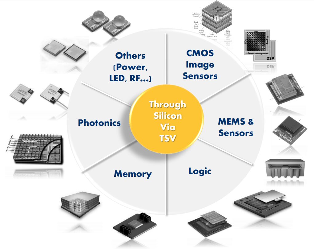
In terms of technology segmentation, 3D and 2.5D integrated circuit packaging technologies encompass various technologies including 3D wafer-level chip-scale packaging, 3D through-silicon vias (TSV), and 2.5D.
Currently, these technologies are playing important roles in cutting-edge technology fields such as high-performance computing, 5G communication infrastructure, and autonomous vehicles. Additionally, 2.5D and 3D advanced packaging technologies are gradually penetrating more embedded applications, such as micro-electromechanical systems (MEMS), CMOS image sensors (CIS), and flash memory, and are expanding their influence into graphics processing units (GPUs), multi-core CPUs, power management units (PMUs), power amplifiers, and field-programmable gate arrays (FPGAs), demonstrating their enormous potential in the future electronic packaging field (Figure 6).
Figure 6: 3D TSV applications are widespread and continue to grow. (Source: Yole Développement)
Although 2.5D/3D packaging technology has not yet formed large-scale applications in RF micro-systems, the number of related research reports is continuously increasing.
Forecasts indicate that by 2028, the market size for 3D and 2.5D integrated circuit packaging is expected to reach $81.67 billion, maintaining an average annual growth rate of about 10.7%. With the continuous advancement of related technologies and the growth of market demand, it is anticipated that in the coming years, 2.5D and 3D packaging technologies will achieve more extensive commercial applications.
Surge in AI Demand Drives Development of Liquid Cooling Technology for Servers
As Chinese AI companies increasingly demand infrastructure construction and computing power supply for intelligent computing centers, the IT equipment energy consumption in such data centers has risen sharply, creating an urgent need for efficient cooling systems to maintain suitable operating temperatures; otherwise, it will pose significant challenges to the cycle management and operation of large model products. On the other hand, governments worldwide are continuously raising energy-saving and emission reduction standards for data centers, accelerating the deployment of green energy-efficient computing power. Therefore, liquid cooling solutions are gradually evolving from being an “optional” choice in previous data center construction and renovation to becoming a “mandatory” option.
Taking the Chinese market as an example, the liquid cooling server market in China continued to grow rapidly in the first half of 2024. The market size reached $1.26 billion, representing a 98.3% increase compared to the same period in 2023, with liquid cooling solutions still primarily based on cold plate technology, accounting for over 95%. It is expected that from 2023 to 2028, the annual compound growth rate of China’s liquid cooling server market will reach 47.6%, with the market size reaching $10.2 billion by 2028.
The internet industry remains the largest buyer in China’s liquid cooling server market in the first half of 2024, accounting for over 60% of the overall market share, with cloud service providers (CSPs) being the most proactive in accelerating the construction of large clusters of liquid-cooled data centers. In addition, telecom operators are gradually implementing the three-year action plan released in 2023 in the “Telecom Operators Liquid Cooling Technology White Paper,” actively exploring infrastructure decoupling solutions, and maintaining rapid growth in the construction of liquid-cooled data centers, which will also be a major source of future demand for liquid cooling servers.
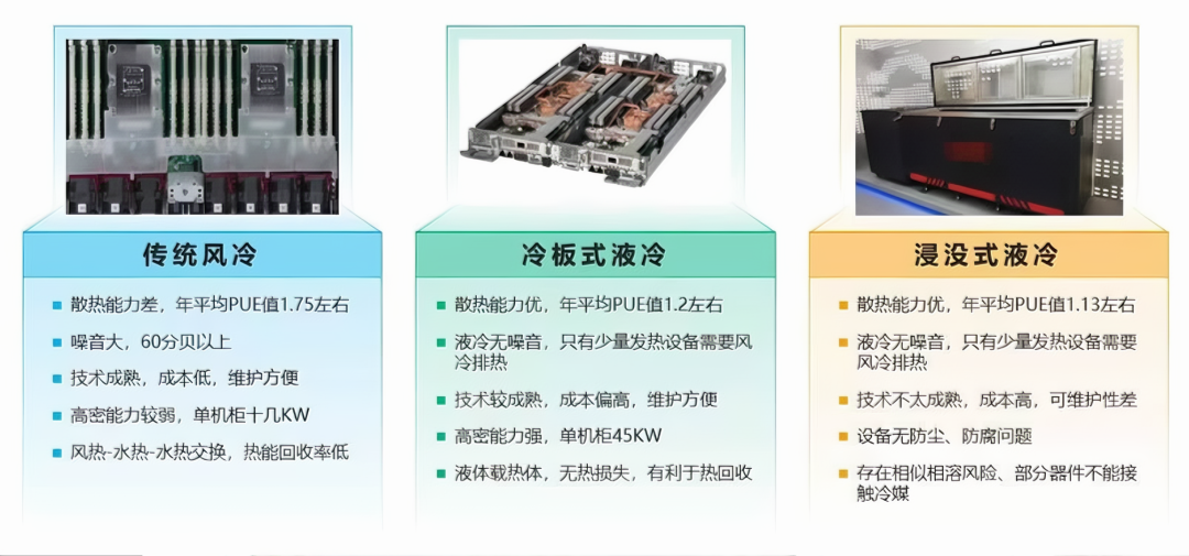
Liquid cooling technology is mainly divided into two types: direct liquid cooling (DLC) and immersion liquid cooling (Figure 7). Direct liquid cooling guides the cooling liquid directly to the heat source of the equipment, removing heat through cooling plates or cooling pipes; immersion liquid cooling completely submerges the entire device in insulating cooling liquid, achieving a broader heat conduction effect, suitable for ultra-high density and high-power equipment heat dissipation. Currently, cold plate liquid cooling, due to its higher technological maturity and complete industrial chain, offers greater construction and maintenance convenience.
Figure 7: Comparison of different cooling technologies—telecom operators are currently mainly promoting cold plate liquid cooling and single-phase immersion liquid cooling technology routes.
Integration, Miniaturization, and Multi-Channel Design Make Biosensors More Powerful
Electrochemical biosensors are analytical devices that combine biological recognition elements (such as enzymes, antibodies, or DNA) with electrochemical transducers, capable of specifically recognizing target biomolecules and converting concentration changes into measurable electrical signals. They have broad application prospects in biomedical, environmental monitoring, and food safety fields.
In recent years, with the continuous improvement of health awareness, electrochemical biosensor technology has made significant progress. The global market size was estimated to reach $2.89 billion in 2023, with a projected compound annual growth rate of 8.0% until 2030.
In the past year, significant technological progress has been made, such as Apple’s non-invasive blood glucose monitoring technology, which is still in the feasible “proof of concept” stage but has brought hope for the development of electrochemical biosensors; teams have also developed portable biosensors capable of detecting extremely low concentrations of biomarkers in serum within a short time. Additionally, advancements in micro-nano manufacturing technology have made integration and miniaturization possible, providing technological support for wearable devices and point-of-care testing (POCT) applications, while the introduction of multi-channel designs allows sensors to detect multiple target substances simultaneously, improving detection efficiency and accuracy.
In the coming year, more new materials are expected to be applied, such as two-dimensional materials, metal-organic frameworks (MOFs), and conjugated polymers, which are expected to become new research hotspots. The currently popular AI technology is also expected to deeply integrate with electrochemical biosensors, achieving intelligent analysis and processing of complex signals through machine learning algorithms, improving detection accuracy and reliability. In specific application areas such as wearable devices, the integration of electrochemical biosensors with smart devices will enable real-time, long-term monitoring of multiple physiological indicators of human health.
However, electrochemical biosensors also face challenges in their commercialization process, such as the need to further improve stability and repeatability to ensure measurement results are reliable. Additionally, cost and strict regulations from global healthcare institutions are also significant factors limiting their large-scale application. This requires the industry to optimize sensor design and manufacturing processes, enhance their performance and stability, while exploring new materials and technologies to reduce manufacturing costs.
Application-Oriented Chip Design: A Ripple Effect
EDA companies have been emphasizing the importance of system design over the past year, or in other words, the era of application-oriented chip design is approaching—not only at the board level but also deeply integrated into system technologies based on specific application requirements.
Taking automobiles as an example, there is a stronger dependence and interconnection between different design domains of modern vehicles. Changes in one part may affect other components, creating a ripple effect. The relationships among components across the entire process of system design, optimization, validation, implementation, manufacturing, and deployment have become incredibly important.
For specific software, a specific chip configuration is required to achieve optimal operating efficiency; changing the software also means corresponding changes in the chip; consequently, this leads to changes in the thermal and other physical characteristics of the chip, necessitating modifications in packaging and systems; the space allocated for batteries may also differ, which in turn affects chassis design, and even impacts the braking system and engine.
Thus, chip design and manufacturing are no longer solely driven by manufacturing processes or merely influenced by advancements in packaging; they are now an integral part of software-defined, application-oriented system design. Chip design needs to be contextualized within the entire system, considering all other components, including assets within the real operating environment.
The digital twin of chip design is situated within the digital twin of the operational system; based on monitoring the chips within the system, understanding the performance of the operational system, and feeding back information into the design phase.
This trend is not only a response to the stagnation or slowdown of Moore’s Law and the increasing demands for computing power due to the digital transformation of society and advancements in AI technology; it is also achievable due to the development of related technologies such as software, AI, IoT, and communication reaching a certain level.