Follow andstar our public account to not miss exciting content

Source:ittbank Edited by: strongerHuangFPGA has been touted as a replacement for ASIC for over a decade by FPGA manufacturers. However, both FPGA and ASIC have their own territories and continue to thrive. What are the differences between these two technologies?
1. Introduction
FPGA (Field-Programmable Gate Array) is a type of integrated circuit that can be configured by the user after manufacturing. It is a further development based on programmable devices like PAL, GAL, and CPLD. FPGAs emerged as a semi-custom circuit in the ASIC domain, addressing the limitations of custom circuits while overcoming the constraints of previous programmable devices with limited gate counts. Today, FPGAs serve as the primary hardware platform for digital system design, characterized by their complete configurability and programmability by users through software, allowing for specific functions to be implemented and reprogrammed multiple times. During modifications and upgrades, there is no need to alter the PCB; changes can be made directly on the computer, transforming hardware design into software development, thus shortening design cycles, enhancing flexibility, and reducing costs.
ASIC (Application Specific Integrated Circuit) is an integrated circuit designed for a specific application. It is tailored to meet the requirements of specific users and electronic systems. ASICs are characterized by their focus on specific user needs and can be categorized into full-custom and semi-custom designs. The highlight of ASICs is their specialization, which allows for faster execution. In summary, ASICs are chips that cannot be purchased off the shelf. For example, Apple’s A-series processors are typical ASICs.
2. FPGA is Reusable
FPGAs utilize the concept of a Logic Cell Array (LCA), which includes configurable logic blocks (CLB), input/output blocks (IOB), and internal interconnections. FPGAs are programmable devices that use small lookup tables (16×1 RAM) to implement combinational logic, with each lookup table connected to the input of a D flip-flop, which then drives other logic circuits or I/O, forming the basic logic unit module capable of both combinational and sequential logic functions. These modules are interconnected using metal wiring or connected to I/O modules. The logic of an FPGA is realized by loading programming data into internal static memory cells, where the values stored in these memory cells determine the logic functions of the logic units and the interconnections between modules or between modules and I/O, ultimately defining the capabilities of the FPGA.
Characteristics of FPGA:
Upon powering up, the FPGA chip reads data from the EPROM into its internal programming RAM. Once configured, the FPGA enters operational mode. When powered down, the FPGA reverts to a blank state, losing its internal logic relationships, allowing for repeated use. Theoretically, FPGAs can be programmed an unlimited number of times.
FPGA programming does not require a specialized FPGA programmer; a general-purpose EPROM or PROM programmer suffices.
FPGAs have a rich set of flip-flops and I/O pins.
They can be quickly produced and modified to correct errors in the program, offering lower costs.
Users do not need to intervene in chip layout and routing issues and can change logic functions at any time, providing flexibility.
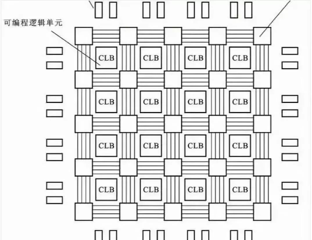
(Basic architecture of FPGA)
3. ASIC Serves VIPs
ASICs are custom-designed, specifically categorized into full-custom and semi-custom.
Full-custom designs can achieve minimal area, optimal routing layout, and best power-speed characteristics, resulting in superior electrical properties. Characteristics include meticulous craftsmanship, high design requirements, long cycles, and expensive design costs.
Semi-custom design methods are further divided into cell-based design methods (CBIC) and gate array-based design methods. Semi-custom designs are mainly suitable for short development cycles, low development costs, and reduced investment and risk for small-scale digital circuit designs.
Characteristics of ASIC:
ASICs are tailored to specific user needs and, when mass-produced, offer advantages over general-purpose integrated circuits, including smaller size, lower power consumption, improved reliability, enhanced performance, increased confidentiality, and reduced costs.
ASICs require longer development cycles and carry higher risks; if issues arise, the entire batch may be rendered useless, making them unaffordable for small companies.
(Basic architecture of ASIC)
4. Design Processes of Both
The complete FPGA design process includes functional description, circuit design and input, functional simulation, synthesis optimization, post-synthesis simulation, implementation and layout, timing simulation, board-level simulation and verification, debugging, and configuration loading.
The ASIC design process (for digital chips) includes: functional description, module partitioning, module coding input, module-level simulation verification, system integration and system simulation verification, synthesis, static timing analysis (STA), and formal verification.
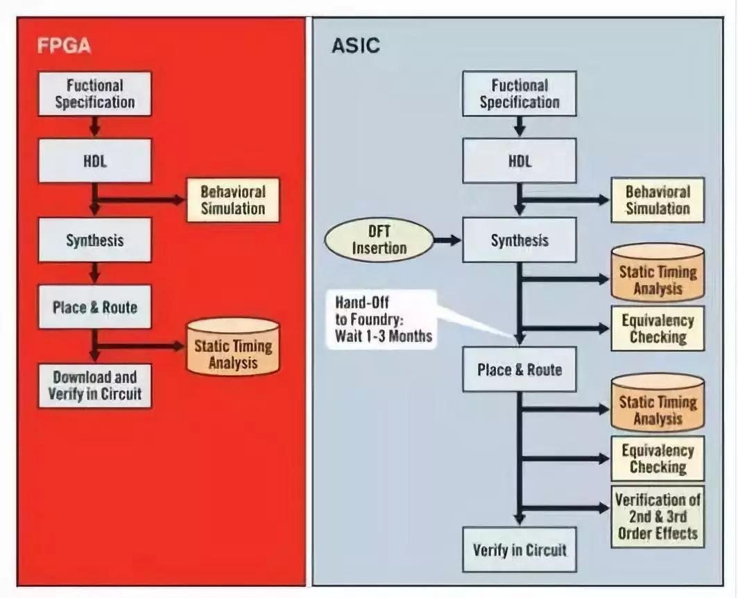
(Design processes of FPGA and ASIC)
It is worth mentioning that during the ASIC design process, FPGAs are often used for prototype verification. FPGA verification is a crucial step in ASIC design, and subsequently, the ASIC version source code must be introduced, along with I/O pads, DFT, power estimation, and other backend processes. Completing FPGA verification can be considered as completing 50-80% of the entire ASIC process.
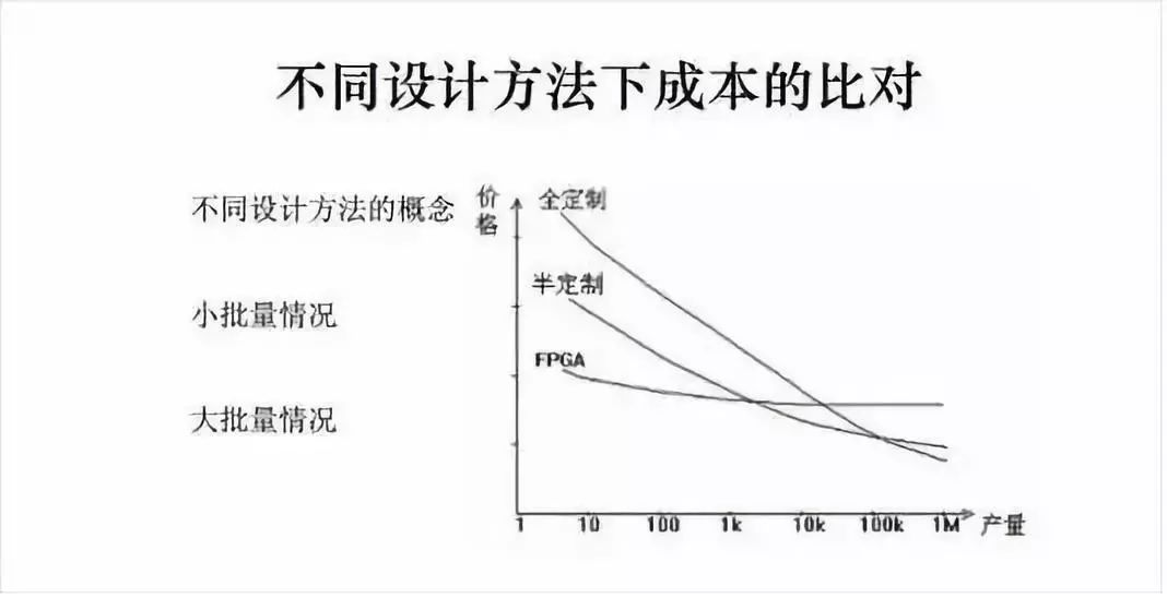
From a design cost perspective, FPGAs have an advantage in small batches, while ASICs excel in large-scale production.
FPGA itself is a chip, but you can modify its internal logic connections and configurations through programming to achieve the desired functionality.Implementing an ASIC is akin to starting from a blank slate; you need code, then synthesis, followed by layout and routing, and finally obtaining GDSII for fabrication.
5. Speed Comparison
With the same process and design, FPGAs are generally slower than ASICs.FPGAs are based on a generic structure, specifically LUTs (lookup tables), which can implement adders, combinational logic, etc. In contrast, ASICs have dedicated adders and comparators, leading to less redundancy in their structure.Moreover, the basic unit of FPGA is the LUT (LUTs form slices, and slices form CLBs – this is Xilinx’s structure), which means that if a large design cannot be implemented with one LUT, it must use two LUTs, and if one slice cannot accommodate it, a CLB must be used. The interconnections between different structures at specific locations lead to wire delays that cannot be ignored.On the other hand, ASICs do not have structural limitations and can be placed very close together, resulting in smaller wire delays and cell delays compared to FPGAs.Of course, LUTs also contain DFFs, and for high-speed designs, a clock is typically inserted after a simple combinational logic operation before proceeding to the next step.
6. Size Comparison
With identical structures, FPGAs are significantly larger than ASICs.FPGAs must be much larger to achieve the same functionality as ASICs, and their maximum frequency is only a fraction of that of ASICs.Thus, FPGAs are still much larger compared to ASICs.
7. Power Consumption
Under the same process conditions, FPGAs consume more power than ASICs.FPGAs, especially those based on SRAM technology with lookup tables (LUTs) that occupy a large silicon area, have significantly higher power consumption compared to equivalent ASICs.
8. Cost Comparison
FPGAs are expensive per chip, but development tools and risks are minimal.In contrast, ASICs incur high costs in fabrication and development tools, with NRE costs becoming quite expensive as processes advance. Unless your chip can be successfully mass-produced on the first attempt, the per-chip cost will be exorbitant!
9. Other Aspects
ASICs are suitable for large projects, while FPGAs are more appropriate for small projects that require rapid market deployment and support for remote upgrades.The main advantage of FPGA technology remains its shorter time to market.
In terms of ASIC advantages, ASICs can operate immediately after power-up, and they offer more packaging options for unit logic size, including certain analog logic. In contrast, FPGAs require time to load configurations into memory and thus cannot operate immediately.Additionally, FPGA packaging is more complex.
Furthermore, FPGAs include I/O interfaces, which are divided into standard I/O and high-speed I/O. High-speed I/O supports interfaces like XAUI and PCIe, which can exceed several Gbps to 10 Gbps.Moreover, various hard IPs are a competitive advantage for FPGA manufacturers, such as POWERPC and ARM hard IPs.This creates a processing platform that integrates CPU and FPGA, combining programmability and reconfigurability.Therefore, although FPGAs have been around for two to three decades, their basic architecture has remained largely unchanged.
10. Positioning of Both
The choice between FPGA and ASIC products should be based on product positioning and design needs. ASIC products are suitable for particularly large designs, such as CPUs, DSPs, or multi-layer switching chips, or for mature technologies with very low profit margins, such as household appliances and other consumer electronics, or for widely used general-purpose devices like RAM and PHY.FPGA products are suitable for medium-scale designs, products that require rapid market entry, or products that need flexible design characteristics, such as PDH, SDH devices below 2.5G, and most interface conversion chips.Ultimately, the specific choice of product for design should be carefully considered based on the product’s positioning.
11. Integration of Both
The most obvious integration is the incorporation of FPGAs into processors, while programmable ASICs are also on the rise.As SoCs become mainstream, the boundaries between the two are becoming less distinct.
12. Final Thoughts on FPGA vs. ASIC Speed
The resources of FPGA, such as LUTs, are fixed; you have exactly what you need and no more.
In contrast, with ASICs, you can manually place every cell or IP resource you use for optimization.
Disadvantages of Fixed FPGA Resources:
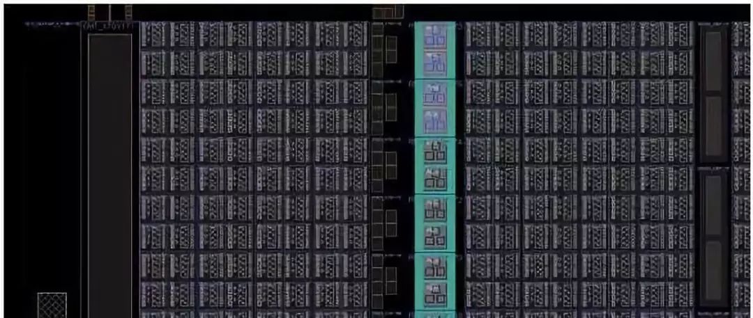
Disadvantage 1:The available resources are fixed and not contiguous, leading to degraded timing for logic that spans regions.This means you cannot place logic as close together as possible.Placing logic close together can reduce line delays and increase speed.ASIC cells can be tightly packed together (as long as DRC rules are not violated).
As shown in the figure below, this is a resource map of an FPGA.
 Disadvantage 2:Your size is fixed.Whether you use 1 gate or 100,000 gates, you are limited to the fixed LUTs available.If your logic is very small, and the FPGA is large, the signal from the I/O to the logic may have to travel a long distance, which also takes time.In extreme cases, if you enter from the top I/O and your logic is at the bottom, the wire length can be quite significant.(Normal designs would not do this.)Additionally, in FPGAs, you have very limited routing flexibility.In ASICs, you can directly widen metal lines, such as doubling the width of clock lines, reset lines, etc.Wider metal lines reduce line delays, which also helps speed.ASIC libraries generally also include high-performance and low-power cells.In critical paths, to improve timing, you can use high-performance cells (which consume more power).For general paths, where timing is more relaxed, you can use low-power cells (which have lower performance).Once you select an FPGA, you are limited to the resources provided; you have no options.ASICs can also utilize useful skew techniques to enhance speed, offering more options than FPGAs.In summary, it is akin to the difference between GPUs and CPUs.GPUs can process images very quickly, but when tasked with other operations, they may struggle.CPUs can handle many types of calculations, including image processing, albeit more slowly.When you design for a specific purpose (ASIC), you can optimize for that goal without compromise.If you aim for versatility (FPGA), you cannot excel in every aspect; trade-offs are necessary.
Recommended Reading:
What domestic IoT operating systems are available, and who dominates?
How to avoid buffer overflow caused by the standard C library?
Command line compilation and downloading with ARM compilation tools Keil and IAR
Follow our WeChat public account “strongerHuang” and reply “1024” to see more content, or reply “join group” to join the technical exchange group according to the rules.

Long press to visit the public account included in the image to follow