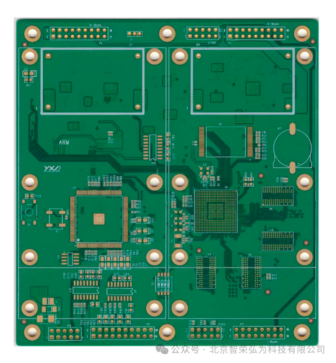
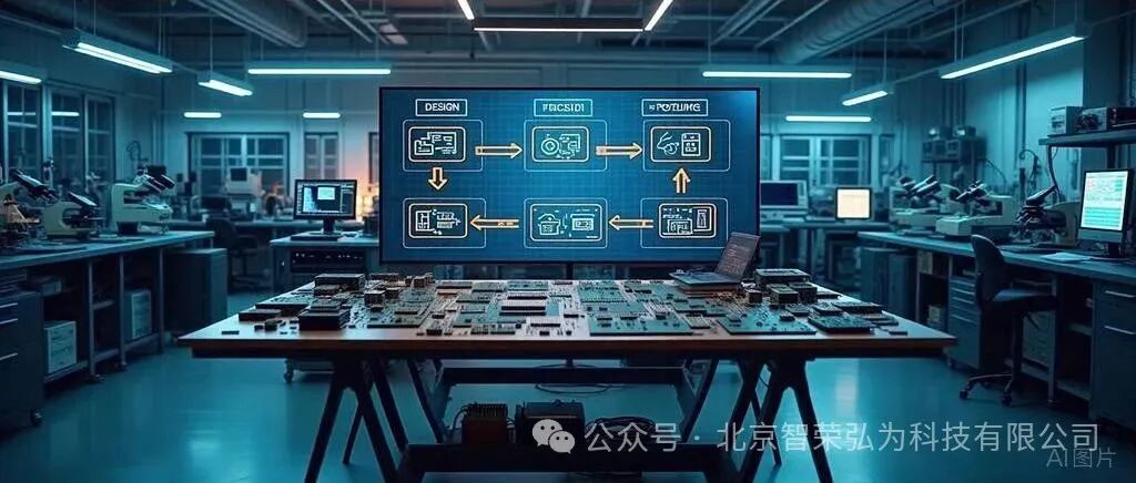
——A Six-Step Journey from “Drawing” to “Physical Product”Step 1: Requirement Planning → Draw the “Design Sketch”· Goal: Clarify what the circuit board is intended to do (e.g., control a motor / transmit data).· Key Decisions:· Board size and shape (square / round / irregular)· How many layers of “sandwich” (single-layer board? double-layer board? multi-layer board?)· Operating environment (high temperature resistant? waterproof?)
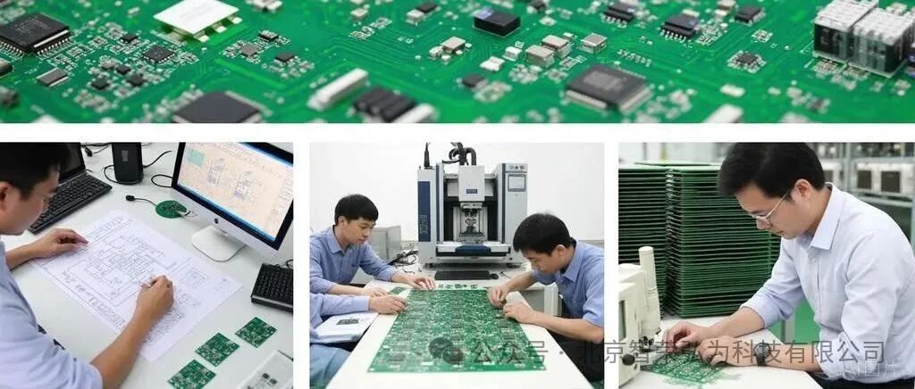
 Step 2: Draw the Circuit Diagram → Connect the “Electronic Building Blocks”· Process:· Select electronic components (resistors / chips, etc.)· Connect component pins with lines like assembling Lego· Generate a Bill of Materials (BOM)
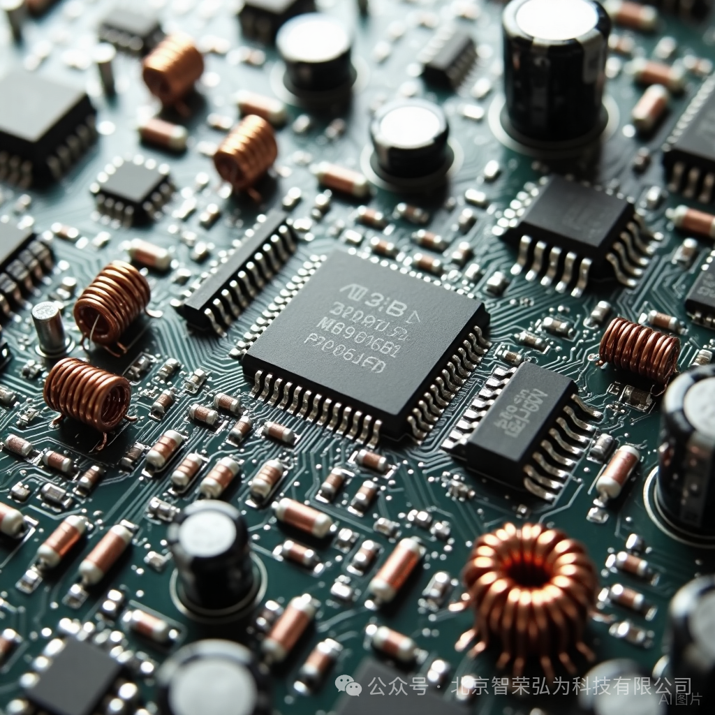
 Step 3: Layout and Routing → Settle the Components· Layout: Place components on the circuit board· Core Principles:1. Heat-generating components should be away from heat-sensitive ones2. High-frequency components should avoid interference sources· Routing: “Build roads” on the board to connect componentsKey Tips: Power lines should be thick, signal lines should not cross or tangle
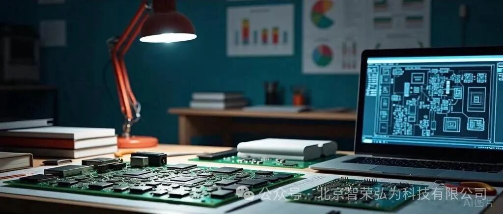
 Step 4: Design Review → Preemptively “Clear Mines”· Software Self-Check: Use tools to check for short circuits, disconnections, and other errors.· Manual Review1. Is there a risk of signal interference?2. Are components too crowded together?3. Can the factory produce it?
 Step 5: Factory Manufacturing → Turn the Blueprint into Reality· Core Processes: Print the circuit diagram → Etch copper foil → Drill holes → Metal plating → Apply green oil → Print characters → Cut the shape· Component Placement: Machines automatically solder components onto the board (SMT process).
 Step 6: Testing and Validation → Ensure “It Works”· Basic Testing: Power on to check for smoke or overheating.· Functional Testing: Simulate actual operation (e.g., pressing a button to see if the light turns on).· Extreme Testing (for some products):1. High and low temperature tests2. Anti-interference tests
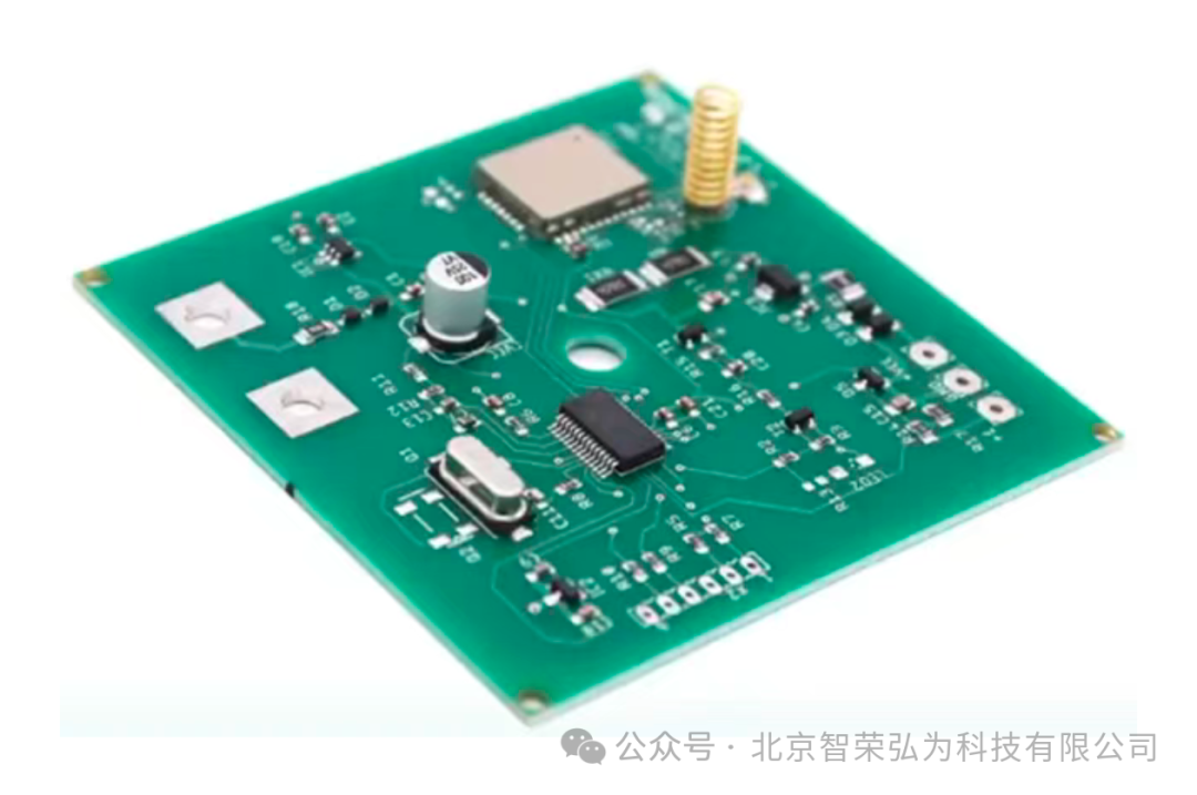 Summary: PCB Development is Like Building a House1. Design Blueprint (circuit diagram)2. Planning Layout (where to place components)3. Construction Team at Work (factory manufacturing)4. Quality Acceptance (testing and debugging)Thank you for reading my article. If you found it helpful, please give me a follow! Let’s chat again next time.