Introduction
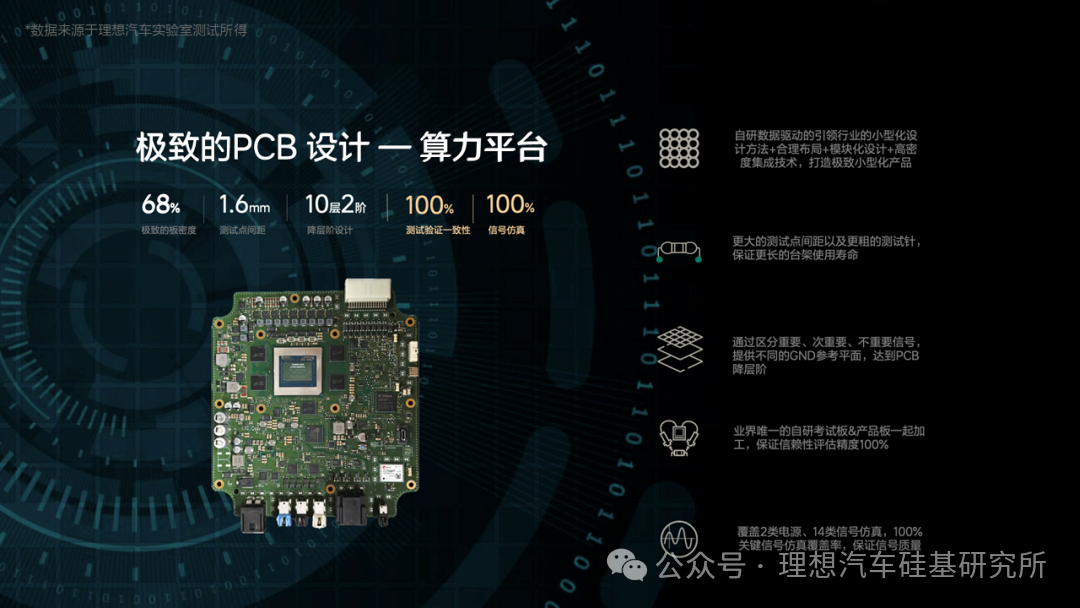
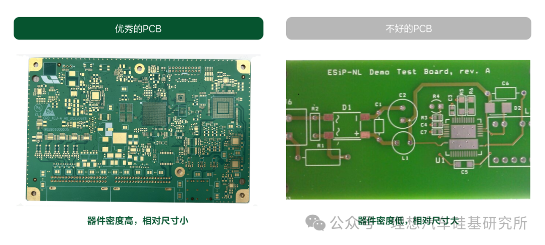
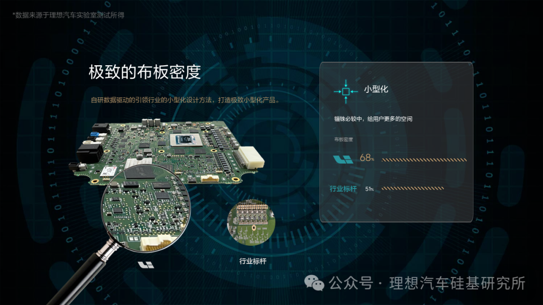
For the “brain” of smart cars—the PCB (Printed Circuit Board), the number of functions that can be integrated per unit area directly determines the technological advancement of the entire vehicle’s electronic architecture. In the Thor-U project developed by Ideal Automotive, the PCB size is 210mm×191mm, with a board density of up to 68%. In contrast, the industry benchmark PCB is larger (341mm×201mm)—close to the size of an A4 paper, but its board density is only 51%. If the electronic components on the industry benchmark PCB are rearranged according to our high-density standard of 68%, Ideal Automotive can achieve the same functionality with a smaller PCB area, saving nearly the space of two smartphones on an A4 sheet. For the limited space in automotive cabins, extreme miniaturization design not only frees up more valuable space but also reserves possibilities for the integration of subsequent innovative functions.
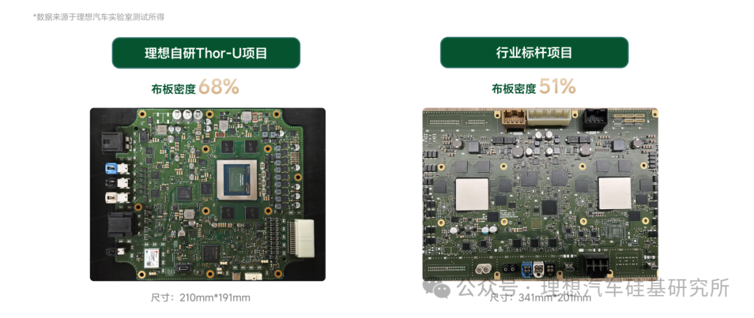
So, what exactly is a PCB? What kind of PCB design can be considered excellent? How does Ideal Automotive achieve a board density of 68%? Let’s uncover the secrets of PCBs.
1. What is a PCB?
PCB stands for Printed Circuit Board. It is an electronic component used for electrical connections and mechanical support. Simply put, it is the skeleton and nerve network of electronic products. Its main function is to provide electrical connections and fixed support between various electronic components, enabling electronic products to function properly.
In our cars, PCBs are usually hidden behind the dashboard, in the onboard computer, camera modules, or inside the seats, making them hard to see, yet they play a crucial role—such as real-time display of vehicle data, controlling the power system, ensuring safety, and supporting rich and interesting in-car entertainment functions, all of which rely on the support of PCBs.
1.1 Intuitive Understanding of PCBs
-
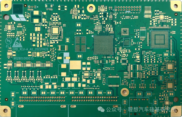
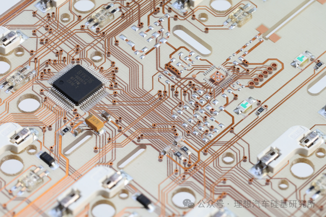
First Impression: Visually, it appears as a green or other colored board with various chips, capacitors, resistors, and complex copper wires soldered onto it.
-
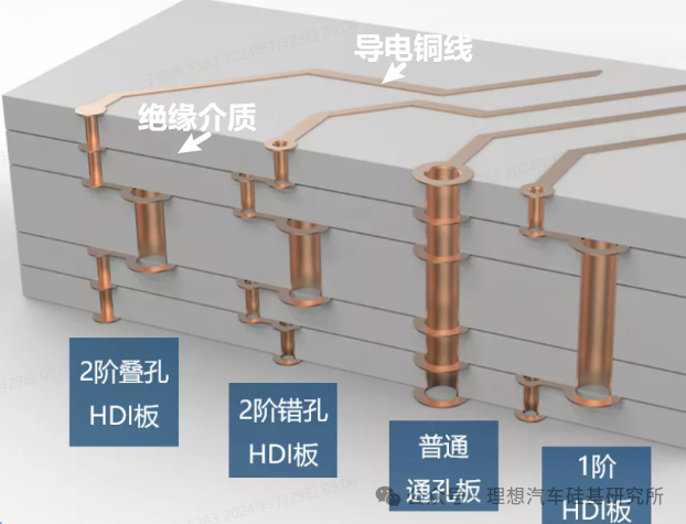
Vertical Slice: If you slice the board like a cake, its interior mainly consists of insulating materials and conductive copper wires.
-
Perspective View: The surface of the PCB will have components installed, with numerous conductive copper wires in each layer. These copper wires serve as the “highways” for information transmission, ensuring that various control commands, sensor data, and power can be transmitted accurately and quickly.
2. What constitutes an excellent PCB design?
In the automotive field, the quality of a PCB directly affects the performance and lifespan of the entire vehicle. Because automotive PCBs need to operate reliably for many years under extreme conditions such as high temperatures, low temperatures, severe vibrations, humidity, and even salt spray corrosion. Therefore, an excellent PCB design must achieve a perfect balance among quality, technology, and space.
2.1 High Quality: Stability Above All
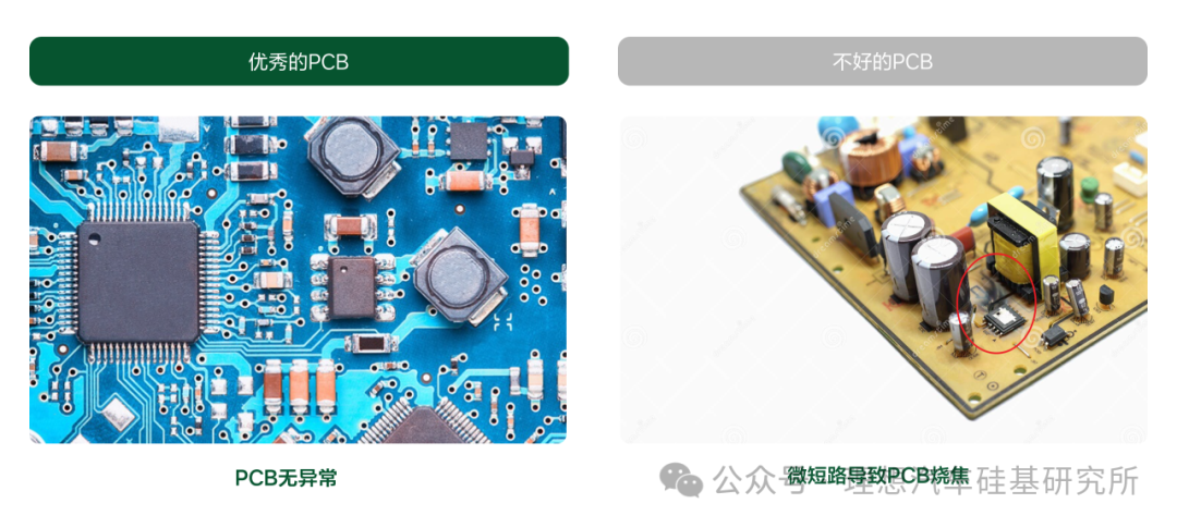
As the brain of the vehicle, the PCB must be extremely reliable, possessing excellent electrical performance to ensure stable and reliable operation throughout the vehicle’s lifecycle. Poor PCB design can lead to internal short circuits, abnormal heating, and in severe cases, component burnout.
2.2 High Efficiency: Stacked Optimization for Ultimate Performance Experience
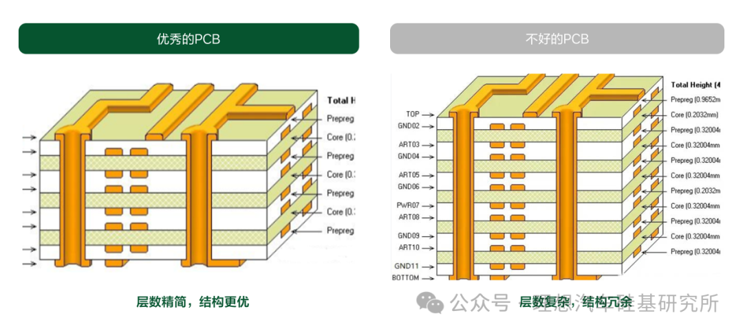
Through scientific stacking design and optimized layer and tier selection, a more compact and reasonable PCB structure can be achieved, resulting in efficient signal transmission, lower energy consumption, and faster response times. High efficiency not only makes the driving experience smoother but also facilitates manufacturing processes and subsequent maintenance.
2.3 Miniaturization: Saving Space, Adding Functions
Space is at a premium in vehicles! To save more space for the entire vehicle, accommodate more vehicle models, and empower the vehicle with more functions, an excellent PCB should be a continuously evolving miniaturized product.
In summary, a truly excellent PCB must be a perfect balance of high quality, high efficiency, and miniaturization.
3. Quality First:
Extremely Strict Testing and Verification Standards
Ideal Automotive has always been committed to the mission of “creating a mobile home, creating a happy home,” placing safety and quality at the core. In the high-quality PCB design and verification phase, we have established a rigorous dual assurance system of <PCB Reliability Design + Testing> and <Board-Level Signal Simulation + Testing> to ensure the product’s outstanding quality and safety reliability.
3.1 PCB Reliability Design and Testing—Quality Assurance Throughout the Lifecycle
Compared to consumer electronics like mobile phones, automotive PCBs face harsher usage environments and longer service life. Therefore, we have higher requirements for the reliability design and testing of PCBs.
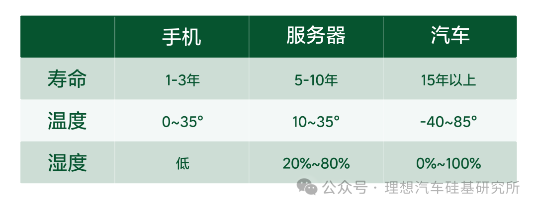
Reliability design and testing, simply put, involves fully considering the various extreme environments that the circuit board may face during the product design and production process, such as high temperatures, low temperatures, humidity changes, electrical stress, and chemical corrosion, and conducting comprehensive verification through a series of rigorous simulations and accelerated aging tests. This approach brings three significant benefits:
-
Improved Product Reliability: By simulating real environments, potential issues can be identified early, enhancing the product’s reliability and stability.
-
Reduced Failure Probability: Reliability testing can effectively lower the probability of product failures during use, providing peace of mind for users.
-
Enhanced Product Competitiveness: High-reliability products are more likely to gain customer trust and enhance market competitiveness.
To ensure that products can cope with various complex working conditions, we integrate reliability concepts into the early design phase, independently formulate and strictly implement material and process standards that have undergone multiple rounds of accelerated aging verification, preventing potential issues from the source and comprehensively enhancing the reliability and stability of the circuit boards. In subsequent product testing, we also adhere to high standards, employing rigorous PCB reliability testing to ensure the long-term stable performance of circuit boards under various environments and electrical loads.
Specifically, our PCB reliability testing includes the following four reliability endurance tests, ensuring PCB reliability throughout its lifecycle:
-
CAF Conductive Anodic Filament Testing: Evaluates the material’s resistance to electrical migration in humid environments.
-
TCT Thermal Cycling Shock Testing: Tests the durability of the circuit board in alternating hot and cold environments.
-
SIR Surface Insulation Resistance Testing: Detects insulation performance to prevent short circuits or leakage.
-
TST High-Temperature Storage Testing: Ensures that the circuit board maintains performance over long periods at high temperatures.
To ensure the scientific and authoritative nature of the tests, we have developed a dedicated PCB test board in the self-developed Thor-U project, which is quite rare in the industry. Additionally, we have adopted a unique process to synchronize the production of test boards with product boards (as shown below), covering various application scenarios such as intelligent driving and regional controllers, achieving complete consistency between product boards and test boards, ensuring absolute reliability. This method is a first in the industry, fully demonstrating our technological innovation capabilities.
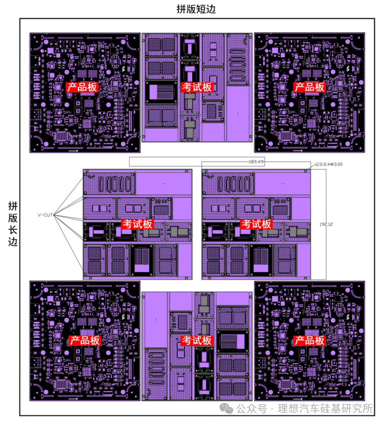
Through the above multidimensional design specifications and rigorous testing, we have built a solid quality assurance barrier for the entire lifecycle of automotive PCBs, ensuring that every circuit board is reliable, durable, and trustworthy.
3.2 Board-Level Signal Simulation and Testing—Risk Preemption, Comprehensive Coverage
In the design of smart car main control PCBs, signal integrity and reliable transmission are crucial. During the design phase, we conduct comprehensive simulations and strict physical tests on all critical power supplies and high-speed signals, allowing us to anticipate and avoid potential risks, ensuring that each circuit board can operate stably and efficiently in practical applications, significantly enhancing system reliability and reducing subsequent development difficulties.
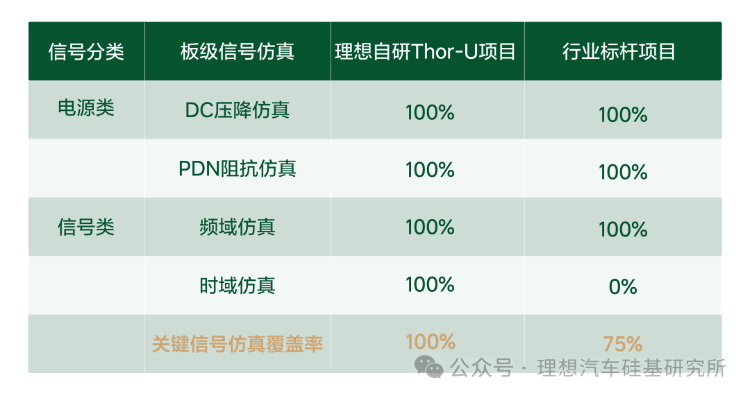
Currently, our simulation capabilities cover two major categories of power supplies and fourteen categories of high-speed signals, encompassing all key power supplies and signals involved in computing platform products, specifically covering the following:
-
Power Supply Category: DC Voltage Drop Simulation and PDN Impedance Simulation
-
High-Speed Signal Category: Time Domain Simulation and Frequency Domain Simulation
Memory Signals: LPDDR5X, UFS, EMMC, OSPI;
Image Processing Signals: GMSL, CPHY, DPHY;
Ethernet Signals: 1000baseT1, SGMII, RGMII, XFI;
Communication Signals: CAN, LIN, USB.
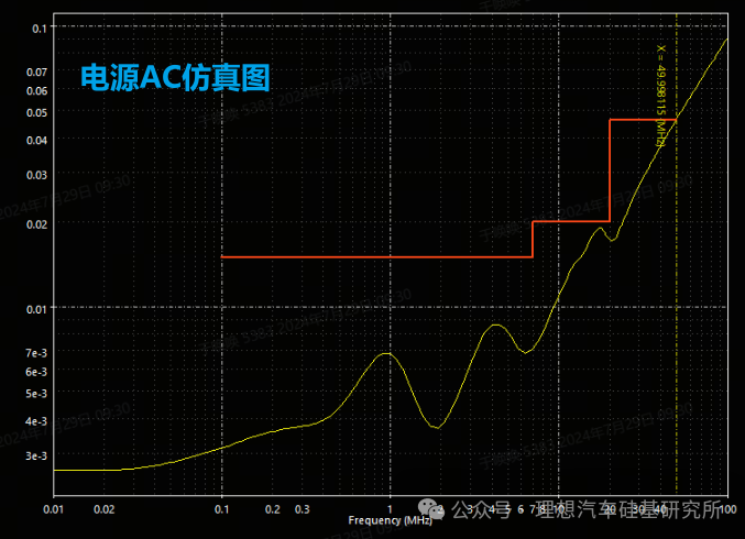
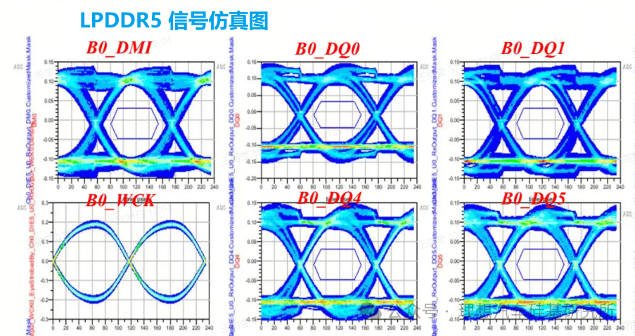
The following diagram visually compares the coverage of board-level signal simulation between our Thor-U project and the industry benchmark project. It can be seen that we have achieved 100% coverage in all key areas, especially in time domain simulation of high-speed signals, far exceeding industry levels.
Moreover, after preemptively addressing risks through simulations during the design phase, we also conducted strict testing on the physical boards. The first version A0 sample of the Thor-U project passed all tests on the first attempt, further demonstrating our leadership and rigor in board-level signal simulation and testing.
In summary, through <PCB Reliability Design + Testing> and <Board-Level Signal Simulation + Testing>, we ensure the signal quality and high reliability of PCBs throughout their lifecycle, thereby safeguarding brand reputation.
4. Focus Breakthrough:
How to Achieve “Extreme Miniaturization”?
Focusing on the goals of high-quality, high-efficiency, and miniaturized PCB design, the computing platform has achieved breakthroughs across the board. Especially in the direction of miniaturization, we have achieved industry leadership through innovative technological paths.
As competition in the new energy vehicle market intensifies, new functions such as autonomous driving, smart connectivity, and augmented reality are becoming increasingly prevalent. These new demands will make the interior space of vehicles tighter. So how can we fit more and more efficient electronic systems into limited space?
In response to spatial challenges, we have been striving for product miniaturization, developing data-driven industry-leading miniaturization design methods to create extremely compact products. This saves more space for the entire vehicle, empowers the vehicle with more functions and selling points, and provides users with a better experience.
Specifically, our miniaturized products feature extreme board density, reasonable layout planning, highly modular design, and high-density integration technology.

4.1 Extreme Board Density
What is board density? Simply put, it refers to how much area on a PCB is actually used for installing components and functional areas. If a board of the same size can accommodate more functions and components, the board density is high, and space utilization is more efficient.
Board density is a comprehensive measure of PCB space utilization efficiency. In pursuit of extreme board density, we have made the following two innovations, achieving an industry-leading board density of 68%.
(1) An innovative calculation method for miniaturization board density, using data to guide design, striving to be the industry TOP.
-
Board Density = (Top Board Density + Bottom Board Density) / 2
Top Board Density = (Top Structure Forbidden Area + Top Component Area + Top Test Point Area) / Single Board Area
Bottom Board Density = (Bottom Structure Forbidden Area + Bottom Component Area + Bottom Test Point Area) / Single Board Area
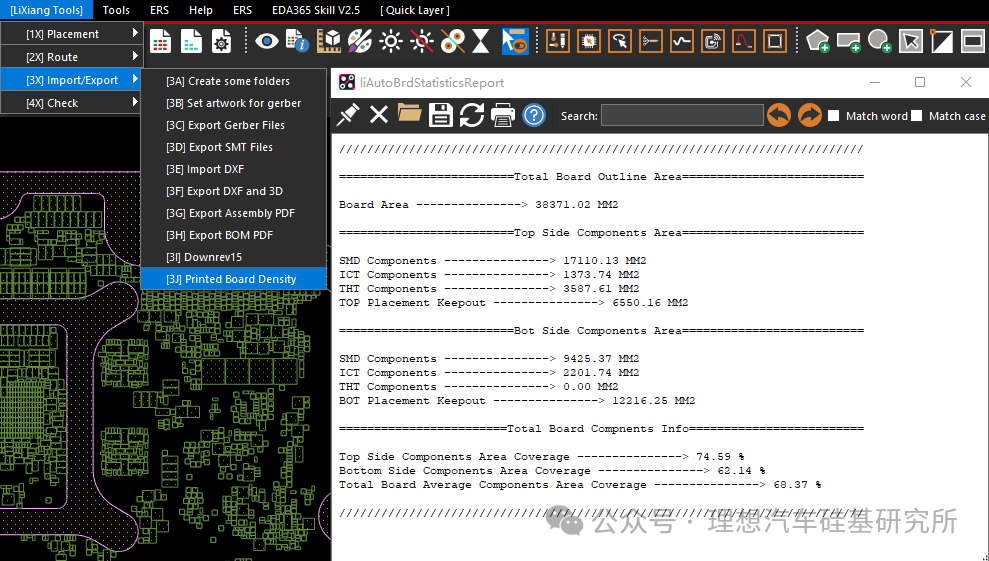
(2) A self-developed auxiliary tool for one-click calculation of board density, guiding miniaturization from measurable to quantifiable, while also reducing the time for assessing single board area to 17% of previous levels (from 3 days to 0.5 days).
4.2 Reasonable Layout Planning
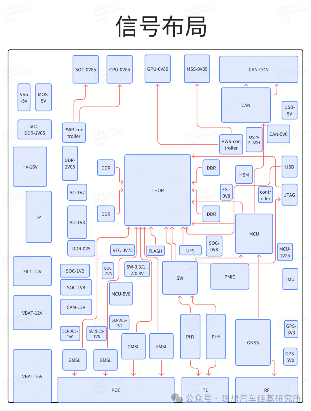
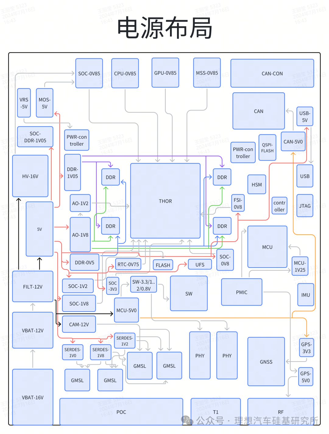
PCB design is not just about “placing components”; it is also about planning the layout early to make subsequent wiring scientific and efficient. To achieve a more compact PCB design, we pursue extreme space utilization during the layout planning phase, ensuring that wiring is planned during the “layout” phase, truly achieving wireless in hand, wired in mind, to fully utilize the entire area of the PCB, ensuring that key signal and power paths are short and cross as little as possible.
4.3 Highly Modular Design
Modular design involves designing circuit units with the same function into standardized, smaller, reusable “independent building blocks”. These “building blocks” can be flexibly arranged like puzzles, which is an important means for us to achieve miniaturization, with specific practices and effects as follows:
-
Designing circuit units with the same function into unified, miniaturized, reusable independent modules, making PCB design more aesthetically pleasing and compact;
-
Modules can be flexibly arranged according to actual needs, maximizing layout space utilization.
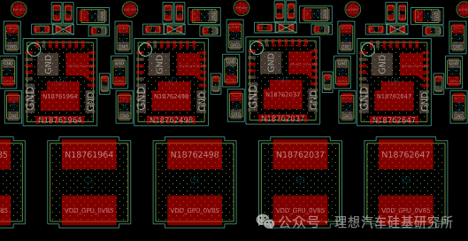
Currently, industry benchmarks also have awareness of modular design, and in terms of module miniaturization, our designs outperform the industry benchmark average.
Our innovation and uniqueness lie in integrating modular design into hardware system construction: improving hardware design and testing efficiency through a modular library management approach.
4.4 High-Density Integration Technology
High-Density Integration (HDI) technology is another core pillar of miniaturized PCBs. It allows us to integrate and realize more complex circuit functions within a limited PCB area. This mainly relies on two technological aspects:
-
Multilayer Stacked PCB Design: Bringing more wiring space through multilayer circuit boards, enabling complex functions to be realized.
-
Advanced Laser Drilling Technology: More precise than traditional mechanical drilling, allowing for higher connection density between layers and more compact component layouts.
This technology represents the current advanced practices in the industry, and our applications have reached corresponding levels, providing solid support for our miniaturization goals.
5. Conclusion
This article introduces the basic concept of PCBs and their core role in smart cars, systematically elaborating on the three key elements of excellent PCB design: high quality, high efficiency, and miniaturization. The article focuses on the innovative practices and significant results of high quality and miniaturization in actual design and application, fully showcasing our breakthroughs and leadership in the field of PCB technology. In the future, as smart cars continue to develop, we will continue to promote PCB technology innovation, empowering more intelligent applications and accelerating the industry towards a higher level.