
Currently, many precision analog-to-digital converters (ADCs) have a Serial Peripheral Interface (SPI) or some form of serial interface to communicate with controllers, including Microcontroller Units (MCUs), DSPs, and FPGAs. The controller writes to or reads from the internal registers of the ADC and reads the conversion codes. The PCB wiring for SPI is simple, and it has a faster clock rate compared to parallel interfaces, which makes it increasingly popular. Moreover, using standard SPI makes it easy to connect the ADC to the controller.
Some new ADCs have SPI, but some have non-standard 3-wire or 4-wire SPI as slaves, as they aim for higher throughput rates. For example, the AD7616, AD7606, and AD7606B series have two or four SDO lines, providing faster throughput in serial mode. The AD7768, AD7779, and AD7134 series have multiple SDO lines used as SPI masters. Users often encounter difficulties when designing the MCU SPI to configure the ADC and read codes.
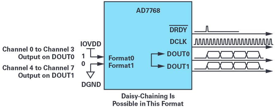
Figure 1. AD7768 used as a serial master with two data output pins (14001-193).
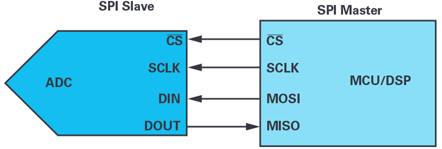
Figure 2. Standard MCU SPI connection with ADC slave.
To initiate SPI communication, the controller must send a clock signal and select the ADC by enabling the CS signal (usually active low). SPI is a full-duplex interface, so the controller and ADC can output data simultaneously through the MOSI/DIN and MISO/DOUT lines, respectively. The controller’s SPI interface allows users to flexibly choose the rising or falling edge of the clock to sample and/or shift data. For reliable communication between the master and slave, users must adhere to the digital interface timing specifications of the microcontroller and ADC chip.
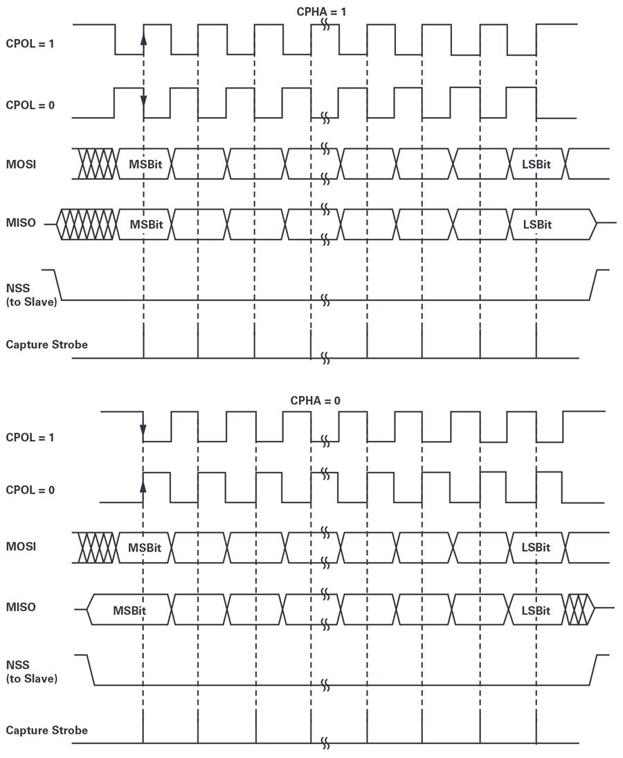
Figure 3. Example of SPI data clock timing diagram.
If the microcontroller SPI and ADC serial interface have a standard SPI timing mode, then users can design the PCB wiring and develop driver firmware without issues. However, some new ADCs do not have a typical SPI timing mode for their serial interface ports. It seems impossible for the MCU or DSP to read data through the AD7768 serial port (a non-standard timing SPI port), as shown in Figure 4.
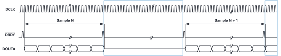
Figure 4. AD7768 FORMATx=1× timing diagram, outputting only through DOUT0.
This article will introduce methods to manipulate the standard microcontroller SPI to interface with ADCs that have non-standard SPI ports.
This article will present four solutions for reading ADC codes through the serial interface:
-
Solution 1: MCU as SPI slave, interfacing with ADC as SPI master using one DOUT line.
-
Solution 2: MCU as SPI slave, interfacing with ADC as SPI master using two DOUT lines.
-
Solution 3: MCU as SPI slave, interfacing with ADC as SPI master using DMA.
-
Solution 4: MCU as both SPI master and slave, reading data using two DOUT lines.
STM32Fxxx series microcontrollers are widely used in many different applications. This MCU has multiple SPI ports that can be configured as SPI master or slave using a typical SPI timing mode. The methods described below can also be applied to other microcontrollers with 8-bit, 16-bit, or 32-bit frames.
The AD7768/AD7768-4 are 8-channel and 4-channel synchronous sampling Σ-∆ type ADCs, each channel having a Σ-∆ modulator and digital filter, supporting synchronous sampling of AC and DC signals. These devices achieve a 108dB dynamic range at a maximum input bandwidth of 110.8kHz, with typical performance of ±2ppm INL, ±50µV offset error, and ±30ppm gain error. Users of the AD7768/AD7768-4 can trade off between input bandwidth, output data rate, and power consumption, selecting one of three power modes to optimize noise targets and power consumption. The flexibility of the AD7768/AD7768-4 makes it a reusable platform suitable for low-power DC and high-performance AC measurement modules. Unfortunately, the serial interface of the AD7768 is not a typical SPI timing mode, and the AD7768 acts as the master of the serial interface. Generally, users must use an FPGA/CPLD as their controller. For example, using the 32F429IDISCOVERY and AD7768 evaluation board. The workaround for SPI line connections is shown in Figure 5. In this setup, all eight channels of data from the AD7768 are output only through DOUT0.
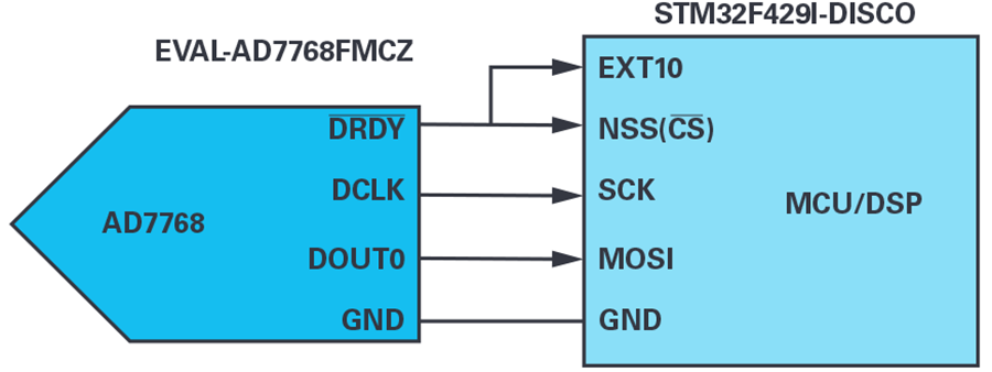
Figure 5. AD7768 outputs data to STM32F429 MCU SPI connection through DOUT0.
Issues to be resolved:
-
Since AD7768 acts as SPI master, the STM32F429I SPI must be configured as SPI slave.
-
The DRDY high-level pulse lasts only one DCLK cycle, which is not a typical CS.
-
After all channel data bits are output, DCLK continues to output while DRDY is low.
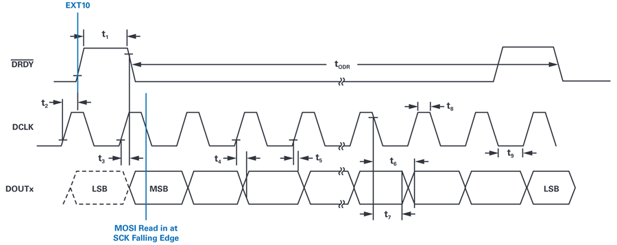
Figure 6. AD7768 data bit reading in timing solution.
-
Configure one SPI port of STM32F429 (e.g., SPI4) as a slave to receive data bits on MOSI at DCLK rate.
-
Connect AD7768 DRDY to STM32F429 external interrupt input pin EXTI0 and NSS (SPI CS) pin. The rising edge of DRDY will trigger the EXTI0 handling routine, allowing the SPI slave to start receiving data bits on the first DCLK falling edge after DRDY goes low. Timing design is crucial here.
-
After receiving all data from channels 0 to 7, the SPI should be disabled to prevent reading additional invalid data, as DRDY will make the SPI slave CS go low while DCLK continues to toggle.
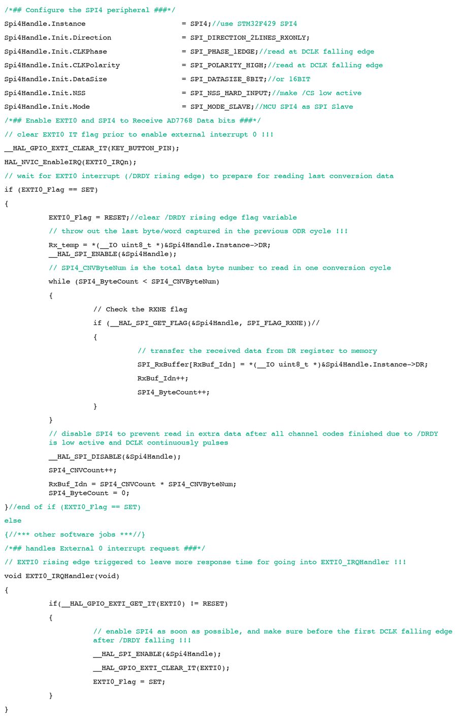
Figure 7. Configuring SPI4 peripheral.
When the software is in interrupt mode, the DCLK running rate can reach up to 4 MHz, achieving an ODR of 8 kSPS. The software should enter the interrupt handler to start SPI within half a DCLK cycle (375 ns). To make it easier for the software to enter the interrupt routine, the MCU can read data on the rising edge of DCLK, providing an additional half DCLK cycle time. However, the minimum propagation delay on DOUTx when t5 DCLK rises to DOUTx is –3 ns (–4 ns when IOVDD = 1.8 V), thus the propagation delay on DOUTx (> |t5| + MCU hold time) should be increased through PCB wiring or buffering.
In the first solution, only DOUT0 is used to output all 8-channel data. Therefore, data reading limits the ADC throughput rate to 8 kSPS. As shown in Figure 1, output channels 0 to 3 on DOUT0 and channels 4 to 7 on DOUT1, reducing data transfer time. The serial line connections are shown in Figure 7. With this improvement, the ODR can easily reach 16 kSPS at a DCLK of 4 MHz.
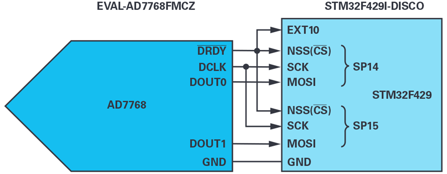
Figure 8. AD7768 outputs data to STM32F429 MCU SPI connection through DOUT0 and DOUT1.
The firmware can operate in polling mode instead of interrupt mode to reduce the time delay from the rising edge of DRDY to enabling SPI to receive data. This allows achieving an ODR of 32 kSPS at a DCLK of 8 MHz.
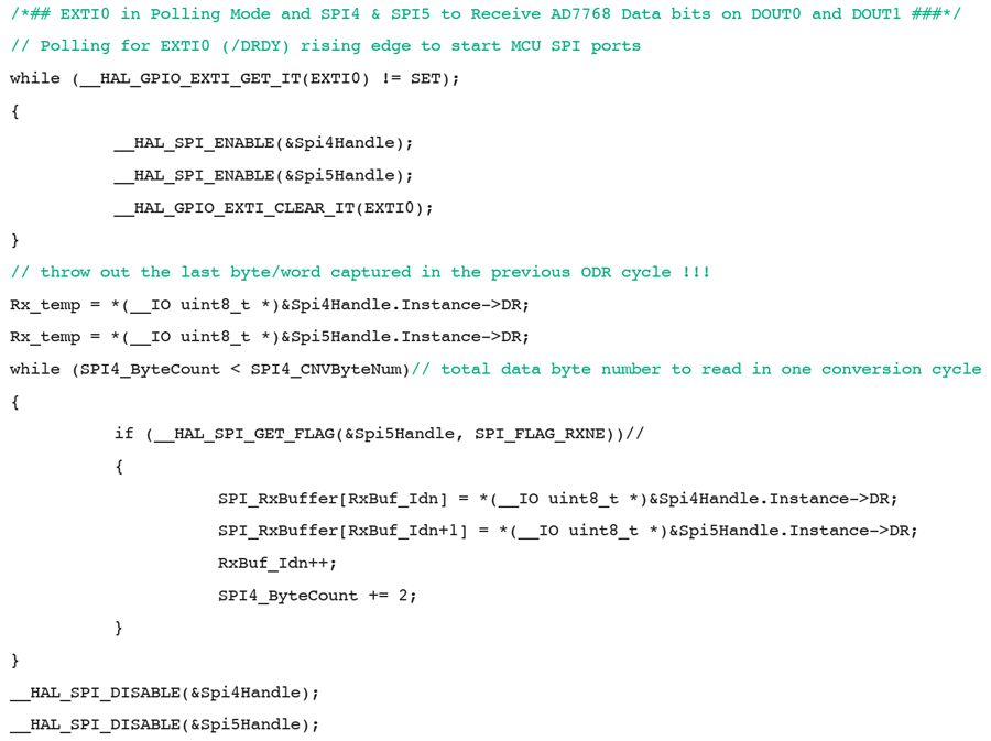
Figure 9. EXTI0 in polling mode, SPI4 and SPI5 receiving AD7768 data bits through DOUT0 and DOUT1.
Direct Memory Access (DMA) is used to provide high-speed data transfer between peripherals and memory, as well as between memory and memory. DMA can rapidly move data without requiring any MCU operations, freeing up MCU resources for other tasks. Below is the design description for MCU SPI as slave receiving data through DMA.
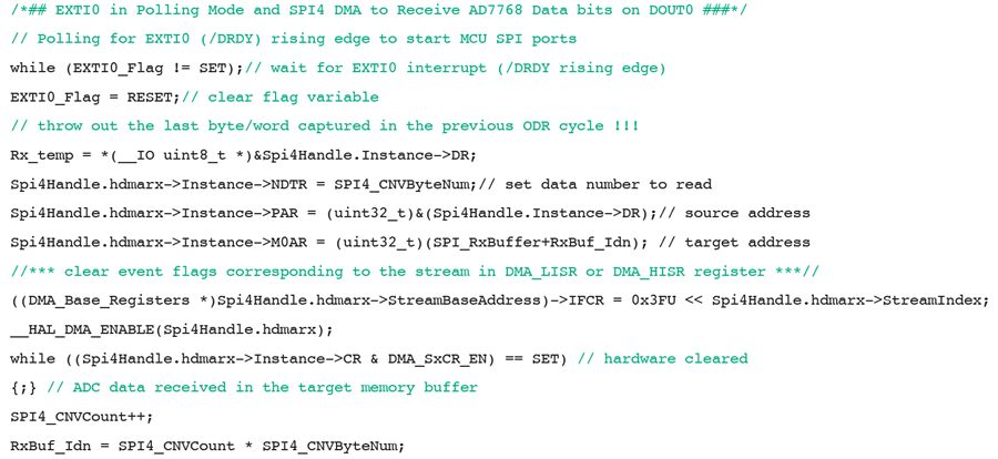
Figure 10. EXTI0 in polling mode, SPI4 DMA receiving AD7768 data bits through DOUT0.
High-throughput or multi-channel precision ADCs provide two, four, or even eight SDO lines for faster code reading in serial mode. For microcontrollers with two or more SPI ports, these SPI ports can run simultaneously to speed up code reading.
In the following use case, the 32F429IDISCOVERY uses SPI4 as the SPI master and SPI5 as the SPI slave, receiving data from EVAL-AD7606B-FMCZ via DOUTA and DOUTB, as shown in Figure 8.
The AD7606B is a 16-bit synchronous sampling analog-to-digital conversion data acquisition system (DAS) with eight channels, each channel containing input clamping protection, programmable gain amplifier (PGA), low-pass filter, and 16-bit successive approximation register (SAR) ADC.
The AD7606B also includes a flexible digital filter, a low-drift 2.5V precision reference voltage source, and a reference voltage buffer to drive the ADC, with flexible parallel and serial interfaces. The AD7606B operates on a single 5V power supply, supporting ±10V, ±5V, and ±2.5V true bipolar input ranges, with all channels capable of sampling at a throughput rate of 800 kSPS.
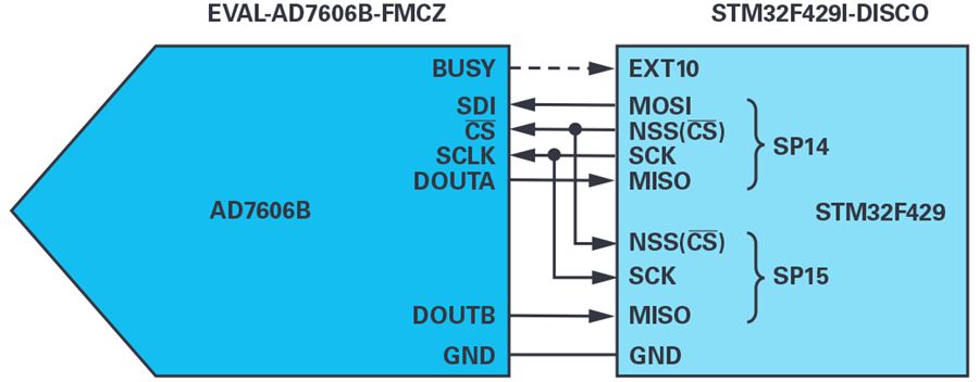
Figure 11. Using MCU SPI in master-slave mode to receive data via DOUTA and DOUTB.
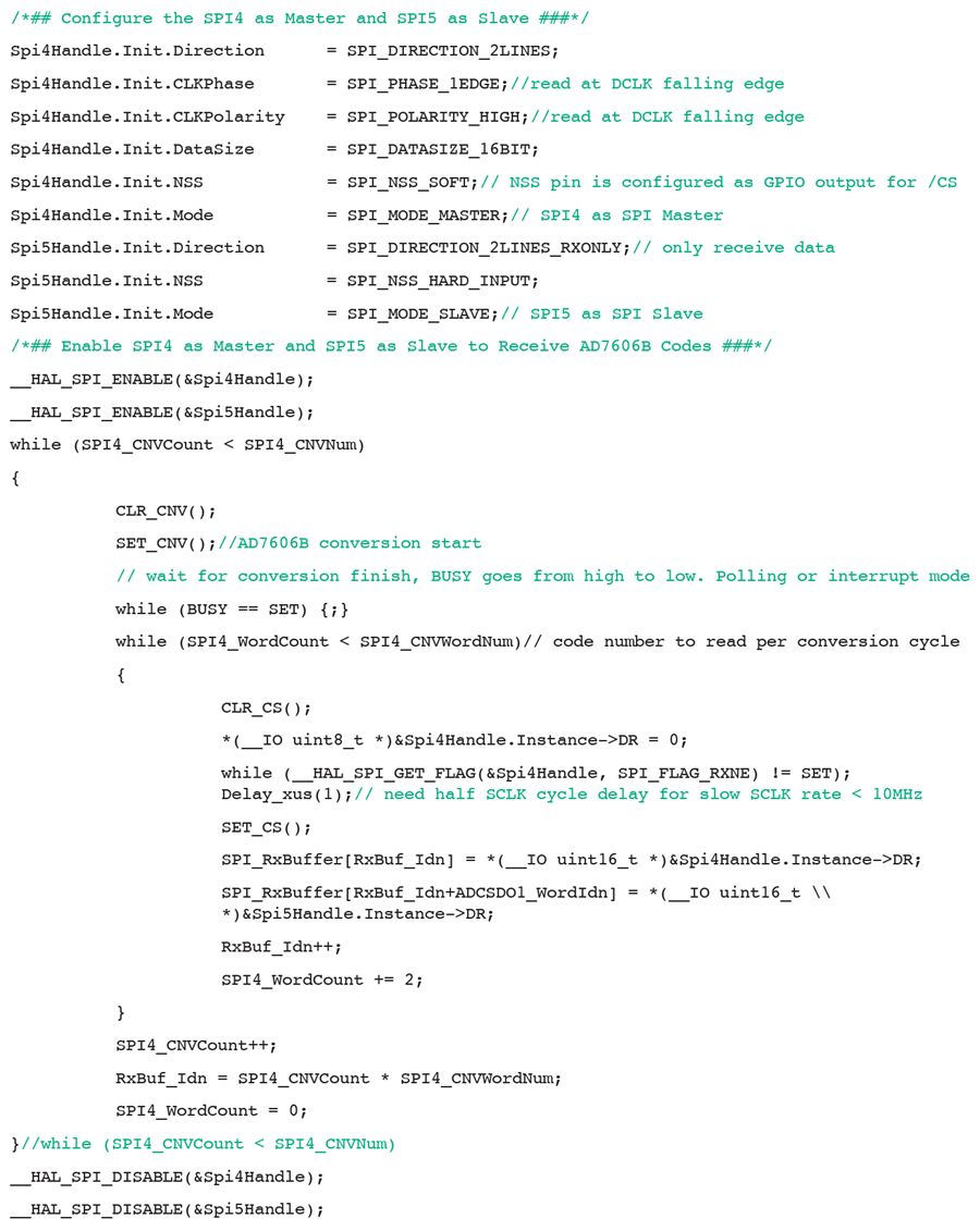
Figure 12. SPI4 configured as master, SPI5 configured as slave.
Figure 13 shows a digital interface screenshot of BUSY, SCLK, DOUTA, and DOUTB while the AD7606B operates at 240kSPS.
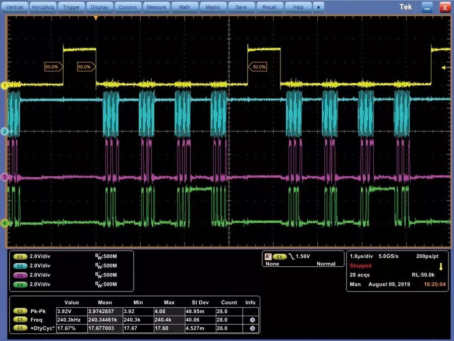
Figure 13. Oscilloscope screenshot of AD7606B BUSY, SCLK, and data on DOUTA and DOUTB.

Conclusion