 1. The AHB system bus is divided into APB1 (36MHz) and APB2 (72MHz), where 2>1 means APB2 connects to high-speed devices.
2. Stm32f10x.h is equivalent to reg52.h (which contains basic bit operation definitions), while stm32f10x_conf.h is specifically for controlling the configuration of peripheral devices, essentially acting as a switch for header files.
3. HSE Osc (High-Speed External Oscillator) is generally 8MHz, and HSI RC (High-Speed Internal RC) is 8MHz as well.
4. LSE Osc (Low-Speed External Oscillator) is generally 32.768KHz, and LSI RC (Low-Speed Internal RC) is approximately 40KHz, providing the watchdog clock and the clock source for the automatic wake-up unit.
5. SYSCLK clock sources have three origins: HSI RC, HSE OSC, PLL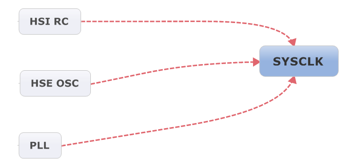
6. MCO[2:0] can provide 4 different clock synchronization signals, PA8.
7. The GPIO port seems to have two diodes connected in reverse series used as clamp diodes.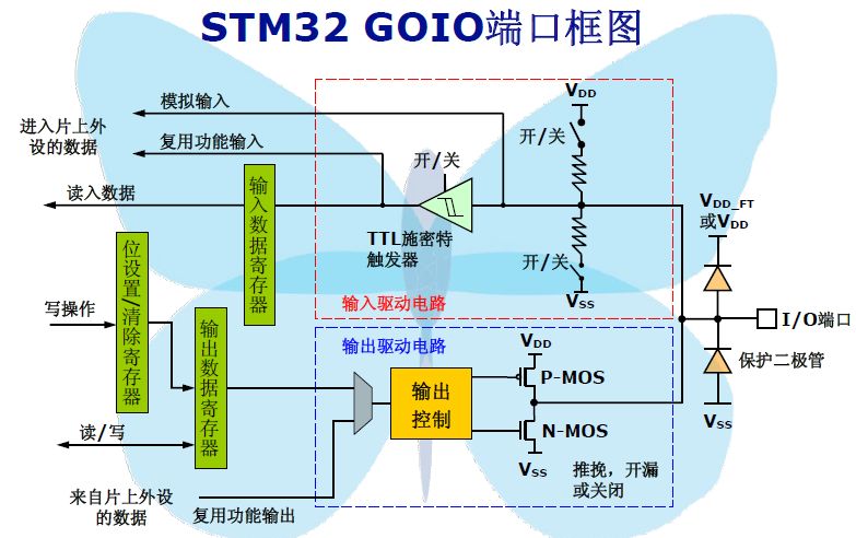
8. The bus matrix uses a round-robin algorithm to arbitrate the system bus and DMA.
9. ICode bus, DCode bus, system bus, DMA bus, bus matrix, AHB/APB bridge.
10. Before using a peripheral, you must set the RCC_AHBENR register to turn on the clock for that peripheral.
11. Data bytes are stored in little-endian format in memory.
12. The memory mapping is divided into 8 large blocks, each block is 512MB.
13. One page of FLASH is 1K (small and medium capacity), large capacity is 2K.
14. The System Memory is locked by ST’s factory configuration, and users cannot edit it, used for reprogramming the FLASH area. Therefore, when programming, we must choose BOOT1 = 0, so that the embedded bootloader can program the FLASH, such as the interrupt vector table and code.
15. The core voltage of STM32 is 1.8V.
16. There are three types of STM32 reset: system reset, power-on reset, backup area reset. Among them, system reset resets all registers except the reset flags in RCC_CSR and values in BKP; the trigger methods include external reset, watchdog reset, software reset, etc.; power-on reset occurs due to the power supply’s power-on/power-off reset or return from standby mode. Resetting occurs except for the values in BKP; backup area reset is triggered by software reset or when both VDD and VBAT are powered off.
17. After the microcontroller resets, all I/O ports are in a floating input state.
18. There are 68 maskable interrupt channels, 16 programmable priorities, and 16 core interrupts, totaling 68+16=84 interrupts. The 103 series only has 60 interrupts, while the 107 series has 68 interrupts.
19. The system startup begins at 0x00000004, 0x0000000 is reserved.
20. (Nested Vectored Interrupt Controller) NVIC is divided into two types: preemptive priority (can be nested) and interrupt priority (sub-priority, cannot be nested). The two priorities are determined by 4 bits. There are sixteen possible allocations: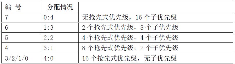
21. Interrupt with preemptive priority 0 can interrupt any interrupt with non-zero preemptive priority; interrupt with preemptive priority 1 can interrupt any interrupt with preemptive priority 2, 3, 4; …; forming interrupt nesting. If two interrupts have the same preemptive priority, the one that occurs first responds first, and they do not nest. If they occur simultaneously (or are waiting), it depends on which has the higher sub-priority; if the sub-priority is also the same, it depends on their interrupt vector position.The original interrupt vector position is the final deciding factor!!!!
22. After power-on initialization, AIRC is initialized to 0, allowing for 16 preemptive priorities, but since all external channel interrupt priority control words PRI_n are 0, the preemptive priorities are the same, and nesting cannot occur.
23. NVI contains ISER[2] (Interrupt Set-Enable Registers), ICER[2] (Interrupt Clear-Enable Registers), ISPR[2] (Interrupt Set-Pending Registers), ICPR[2] (Interrupt Clear-Pending Registers), IABR[2] (Active Bit Registers), IPR[15] (Interrupt Priority Registers). Among them, ISER and ICER are the interrupt enable and disable registers, both written 1 to enable/disable interrupts. Why write1? Why use two registers instead of one to represent the interrupt enable/disable state? Due to hardware, writing0 is more complex and may change the state of other bits, so using1 to indicate on or off is more reasonable.
24. Interrupt flag bits need to be cleared manually.
25. General steps to configure peripheral devices: 1. Turn on port clock. 2. Define the initialization structure and initialize it. 3. Call
26. The parity check for serial ports: If parity is used, then USART_InitStructure.USART_WordLength= USART_WordLength_9b; the length of this data must be set to 9 bits!
27. The ADC’s regular group can customize the conversion channel order and the number of conversion channels. In practical applications, sometimes it is desired for certain channels to have high priority and force an interruption during the conversion of the regular group to perform conversion on another channel; this group of channels is called the injection group.
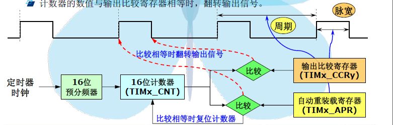
28. The timer’s output compare mode: Timing (freeze, do nothing, ordinary timing), Active (OCxREF output high level effective), Inactive (OCxREF output low level), Toggle (flip level after comparison success).
29. The STM32 timer counts from 0, satisfying certain conditions, giving flag bits (such as match success, time update, overflow, etc.) and then starts counting from 0. This is different from the 51 series.
30. OCx=OCxREF+polarity
31. Auto-reload register and shadow register: The former is equivalent to the overflow setting value in the 51 series. The shadow register, as the name implies, is a copy of the register. The shadow register is what takes effect, while the programmer manipulates the auto-reload register. If the APPE bit is enabled, it indicates that the value of the auto-reload register will only be written to the shadow register after the next update event occurs. Otherwise, writing to the auto-reload register will immediately update the value to the shadow register.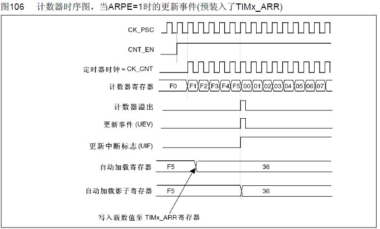
32. RCC_PCLK1Config(RCC_HCLK_Div4); The 4 division of PCLK1 sets the timer reference clock.
33. Timer configuration: RCC, NVIC, GPIO (OC output or PWM), TIMx.
34. General timers can output 4 different PWM, while advanced timers can output 4 different PWM and also 3 complementary PWM signals (for driving three-phase motors), totaling 7 channels. Thus, STM32 can produce 30 PWM = 7*2+4*4.
35.
36. The clock source of the advanced timer hangs on APB2, while the general timer hangs on APB1. AHB (72MHz) → APB1 divider (default 2) → APB1 clock signal (36MHz) → multiplier (*2) → general timer clock signal (72MHz). If APB1 has no division, then the clock signal frequency of the general timer equals the clock frequency of APB1, without the above multiplier*2 process. TIM_SetAutoreload() is used to change the frequency of PWM, and TIM_SetCompare1() is used to change the duty cycle.
37. Brushed motors generally have larger starting torque, while brushless motors have smaller starting torque but larger running torque. Brushed motors use mechanical current commutation with brushes, while brushless motors determine the rotor’s motion position and direction through Hall sensors, returning to the control loop.
38. Dead time is necessary because it concerns short circuit issues. Thyristors require dead time to completely turn off the circuit when switching directions.
39. The braking function is used to automatically provide external motors with emergency braking when issues arise in the control loop, reflected in PWM by continuously providing a fixed duty cycle? (Is it also for three-phase drive?)
40. PWM output is best done using PWM mode; other comparison output modes will gradually change phase and become imprecise.
41. Reading and writing to FLASH requires unlocking first and then locking. Writing 0 is easy, writing 1 is difficult.
42. There are two ways to download programs: one is ICP (In-Circuit Programming), suitable for programming under JTAG or SWD protocols. The other is IAP (In-Application Programming), suitable for many interfaces (USB, serial, CAN) to download to memory. IAP allows reprogramming of FLASH while the program is running.
43. FLASH is divided into main memory (where user program code is stored) and information blocks (boot code). In addition, there is a part called system memory, which cannot be operated by the user and is fixed after ST’s production for the system’s power-on boot program.
44. When writing to FLASH, you must not read; if there is a read operation, it will lock the bus.
45. When operating FLASH, HSI must be enabled.
46. STM32 has two watchdogs (IWDG independent watchdog with independent clock, WWDG window watchdog derived from APB1).
47. The maximum frequency of SPI is 36MHz (fpclk/2).
48. TIM1 and TIM8 advanced timers need to configure the main output function (CtrlPWMOutputs) to output PWM. Other general timers do not need such configuration. However, TIM6 and TIM7 do not have PWM output functionality.
49. Code refers to the program code section.
RO-data represents program-defined constants (e.g., const temp, etc.);
RW-data represents initialized global variables.
ZI-data represents uninitialized global variables, and variables initialized to 0.
Code, RO-data, RW-data…………..flash
RW-data, ZIdata……………….RAM
During initialization, RW-data is copied from flash to RAM.
50. STM32F103ZET6 has 144 pins (Z for 144), among which 112 pins are available for I/O (7X16=112, ports A-G).
51. ARM only produces standard cores and does not produce chips. Companies like ST and TI purchase cores from ARM and then add their own bus structures, peripherals, memory, and reset/I/O to create their own chips.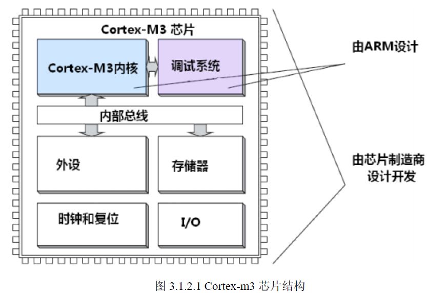
52. The CMSIS standard is used to exchange information between the upward user layer and the underlying hardware layer. This architecture can be defined by oneself, but then there will be no standard. Therefore, the CMSIS standard is enforced for chip design. In simple terms, the function names for system initialization are defined by CMSIS as SystemInit(), GPIO_ResetBits(), etc.
53. Port multiplexing and port remapping are two concepts: the former requires enabling the corresponding port and its functional clock. The latter requires turning on the AFIO clock and then performing port remapping using GPIO_PinRemapConfig().
54. Downloading programs can only use serial port 1, which must be noted in hardware design!
55. The J-TAG debugging frequency is generally set to 2MHz, while the SWD debugging frequency can be set to 10MHz.
56. The SysTick interrupt implementation can be done in two ways: polling and interrupt method. It is recommended to use polling; the interrupt method may have issues and occupy resources.
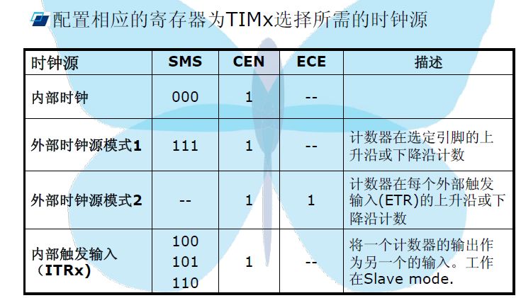
57. Some I/O pins are 5V compatible. The maximum drive current and sinking current for a single I/O is 25mA. The total current for the chip is 150mA.
58. KEIL supports bit-field operations, allowing the definition of bit-field structures using bit-field knowledge in C, and then performing individual bit operations on specific registers.
59. Regarding the setting of internal pull-up and pull-down resistors: If one end of the external button is grounded, then it needs to be set to pull-up resistor. (The reason is that when the button is not pressed, due to pull-up, the input is high; when pressed, due to external grounding, the input is low.) Similarly, if the other end of the external button is connected to a high level, then it needs to be set to pull-down resistor.
60. The difference between serial port interrupt TXE and TC is quite clear: one is the transmit register empty flag, and the other is the transmit complete flag. Because the serial port first needs to shift the data from the transmit register to the shift register (shadow register) before sending it serially. So when the transmit register DR is empty, it indicates that data might still be sending out. But transmit complete is different; it is set after the shift register has shifted all the current data (i.e., after sending the stop bit). Thus: TXE allows the program more time to fill theTDR register, ensuring that the data stream is uninterrupted.TC lets the program know the exact time when sending ends, which is beneficial for controlling the timing of external data flow.
61. The window watchdog, as its name suggests, has a window, with the horizontal coordinate being time, meaning that the register must be refreshed within a specified time range, otherwise the microcontroller resets. The upper limit of the window is set by the user W[6:0], and the lower limit is fixed at 0x40Twwdg=(4096×2^WDGTB×(T[5:0]+1)) /Fpclk1; Twwdg is the timeout in ms, and Fpclk1 is the APB1 clock in KHz.
62. The TIMx general timer has 4 independent channels, which can be used for: input capture, compare output, PWM generation, single pulse mode output.
63. The clock sources for the timer are 4: internal clock (CK_INT), external clock mode 1 (TIx), external clock mode 2 (ETR), internal trigger mode (ITRx, which is used for timer synchronization).
64. Timer interrupt overflow update time: Tout=((arr+1)*(psc+1))/Tclk, where ARR is the auto-reload register (1~65535), PSC is the prescaler, and TCLK is the input clock frequency (MHz).
65. The difference between PWM1 and PWM2 modes lies only in the 180-degree phase. The former is high when the latter is low. It seems quite redundant; the OCxREF polarity can achieve this function.
66. Timer input capture has a filter, which serves to filter the signal. When capturing external signals, the signal may be unstable, requiring filtering: when detecting an external input, it needs to sample continuously N times; if determined to be high/low, then trigger the response interrupt (if enabled).
67. The capacitive touch screen principle: detects whether it is pressed through the charging and discharging curve differences. In actual experiments, the TPAD can be replaced by a copper-clad area, determining whether pressed through the capacitor’s charge and discharge constant.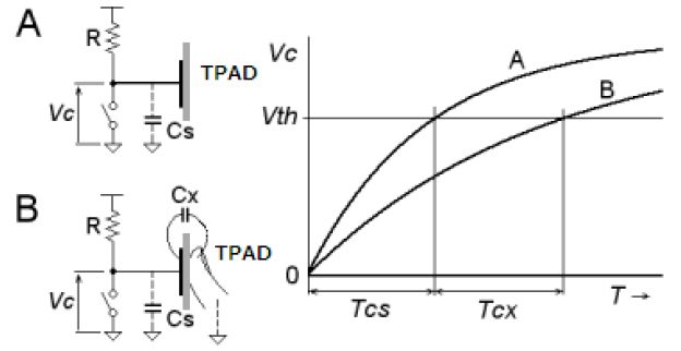
68. OLED, or Organic Light-Emitting Diode, is also known as Organic Electroluminescence Display (OELD). The following image shows the correspondence between OLED’s GRAM and the screen: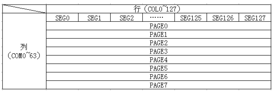
PAGE2 is listed separately: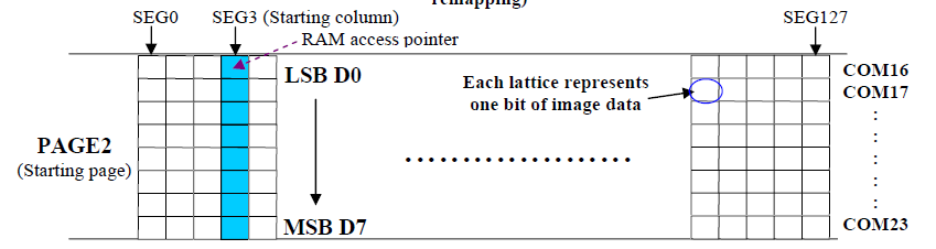
69. USART can control SPI devices. However, the maximum frequency is only 4.5MHz.
70. Issues to note when using I/O ports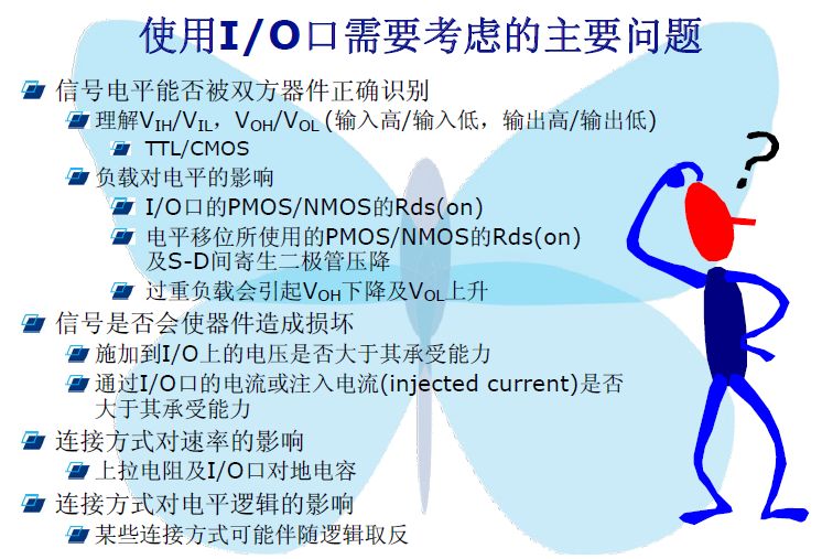
71. The ADC’s Vref+ and Vdda with VSS, Vref- must have high-quality filter capacitors, placed close to the microcontroller.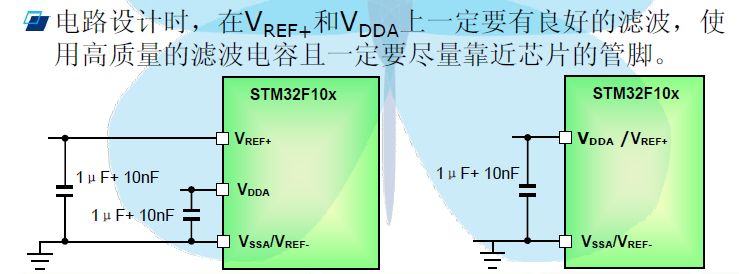
72. The ADC is divided into regular groups and injection groups, the former has 16 channels, and the latter has 4 channels. Moreover, the 16 channels share one value register, while the injection group’s 4 channels each have one value register.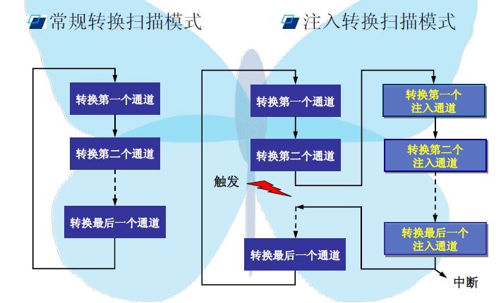
73. The higher the sampling frequency, the lower the input impedance requirement.
74. The shortest cycle for STM32 to enter an interrupt is 6 cycles.
75.
76.
77. FSMC, or Flexible Static Memory Controller, can interface with synchronous or asynchronous memory and 16-bit PC memory cards. The STM32’s FSMC interface supports various types of memory, including SRAM, NAND FLASH, NOR FLASH, and PSRAM.
78. The FLASH memory in common USB drives comes in two types: NAND flash and NOR flash.
|
NAND FLASH |
NOR FLASH |
|
Cannot directly execute code inside |
Can directly execute code inside |
|
Fast write and erase speed |
Slow write and erase speed |
|
Reading speed slightly slower |
Reading speed slightly faster |
|
Erase cycle 1 million times |
Erase cycle 100 thousand times |
|
Low cost, high capacity |
High cost, low capacity |
|
Generally serial interface |
Has SRAM interface |
79. TFT can be operated as external SRAM during operation. If the microcontroller has an FSMC interface, it can control the NOR FLASH’s SRAM interface, resulting in very fast speeds.
80. The STM32’s FSMC has 4 blocks of 256MB storage, addressing a total of 1GB of external storage space.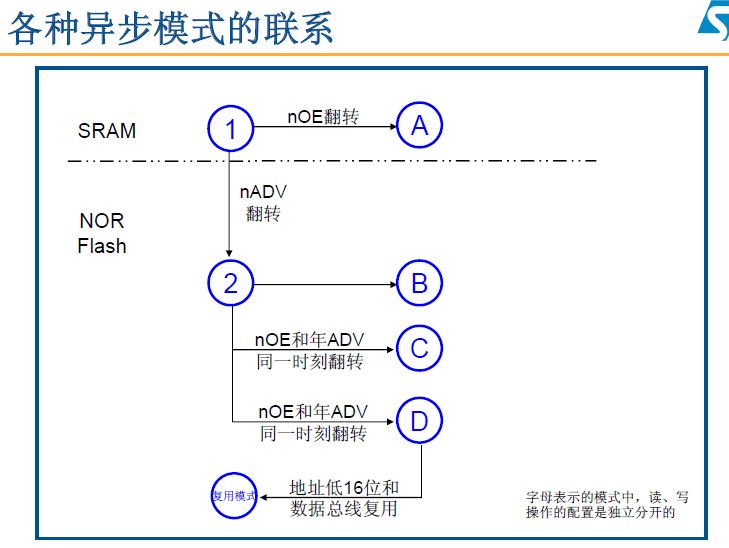
81. Inside the STM32, one end of the FSMC is connected to the Cortex-M3 core via the internal high-speed bus AHB, while the other end connects to the external bus for extended memory. The core sends access signals to the external memory to the AHB bus, which FSMC converts into signals that conform to the external memory communication protocol and sends them to the corresponding pins of the external memory for data exchange.
82. The settings for DATASET and ADDSET in FSMC must refer to the timing diagram of the external memory. Generally, DATASET refers to the data setup time, which is the duration from the start of the read/write signal to the stop of the read/write signal (data is stored on the rising edge). ADDSET refers to the address setup time, which is the time from chip select to read/write operation; this applies to SRAM. If controlling a TFT, there are no address lines, so ADDSET refers to the time from the end of the read/write signal to the transition of the RS level.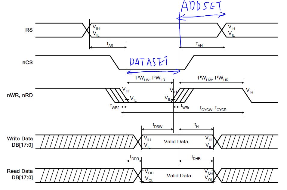
83.
84.
85. The three configuration registers in FSMC are: FSMC_BCRx (Chip Select Control Configuration), FSMC_BTRx (Chip Select Timing), FSMC_BWTRx (Chip Select Write Timing).
86. RTC clock configuration must use the BKP register, which does not change values during microcontroller reset, power reset, or standby wake-up mode; it is powered by VDD, and after VDD is cut off, it automatically switches to external VBAT power.
87. To modify the BKP register value, the write protection flag must be cleared. BKP register is automatically write-protected at power-on.
88. The STM32 has three power-saving modes: 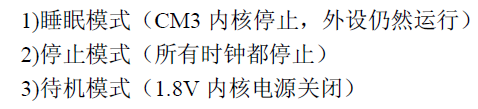 The power consumption in the three power-saving modes decreases from top to bottom, with standby mode’s current being only2uA.
89. Waking the microcontroller from standby mode is equivalent to resetting the microcontroller, but the power register’s value will have a flag indicating that the microcontroller was awakened, not reset.
90. The ADC’s clock should not exceed 14MHz; otherwise, conversion accuracy will decline. The maximum conversion rate is 1MHz, meaning a conversion period of 1us (14MHz, the sampling period is 1.5 ADC clock cycles).
91. Tcovn= sampling time + 12.5 cycles. The longer the sampling time chosen, the higher the accuracy, but the conversion rate declines; this is a trade-off.
92.
93. Taking ARM7TDMI as an example, T represents the Thumb instruction set, D indicates support for JTAG debugging (Debugging), M refers to a fast multiplier, and I corresponds to an embedded ICE module.
94. MMU serves as a watershed mark between embedded processors and application processors. A processor with a memory management unit can be identified as an application processor. Thus, the difference between M series and A series processors lies in that the A series processors have an MMU unit for memory module management.
95. ARM processors have two states: ARM state and Thumb state.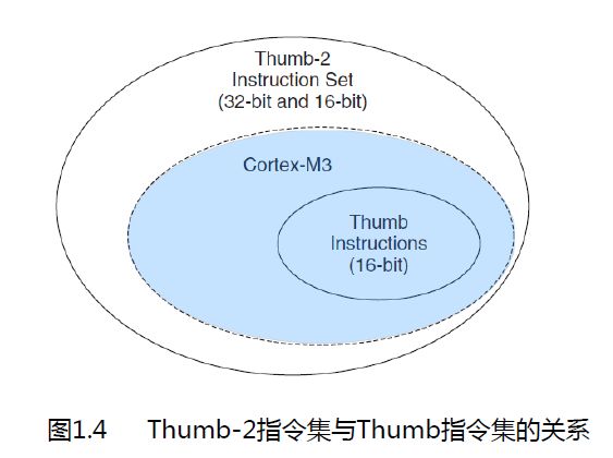
96. This image explains everything: the Thumb2 instruction set has achieved a great feat: integrating 16-bit and 32-bit instruction sets, with very strong compatibility! (This means that CM3 does not support certain 32 bit ARM instruction sets??)
97.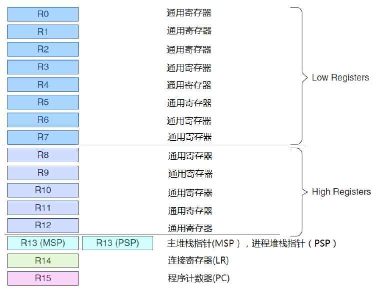
98. The MSP is the stack pointer used after system reset, while the PSP is used by user code. The two stack pointers are 4 byte aligned!!
99. In the field of ARM programming, any event that interrupts program execution is collectively referred to as exceptions.
100. Because of the existence of LR (link register), it supports one level of subroutine calls without pushing to memory, greatly improving execution speed.—àThis means that during programming, one-level calls will not consume much time, unless it is a two-level call!
101. The processor has two operating modes: handler mode and thread mode.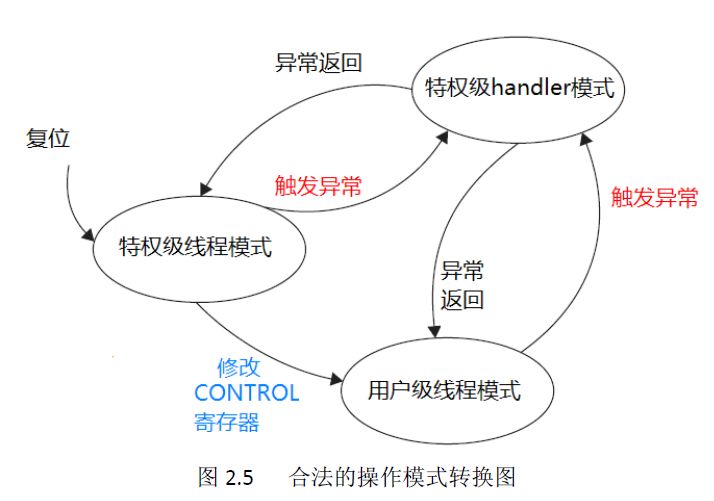 The processor also has two privilege levels: privileged level and user level. This image explains everything: after reset, the system enters privileged thread mode; if an exception occurs, it enters privileged handler mode to handle exceptions or interrupt routines, then returns to privileged thread mode. By modifying the CONTROL register, it can enter user-level thread mode.
102. The two advanced timers TIM1 and TIM8 are connected to the APB1 bus.
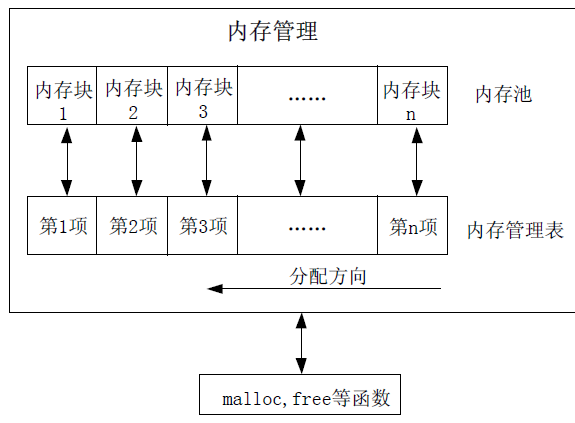
103. STM32’s external interrupts are distinguished by groups, meaning that the microcontroller cannot distinguish which triggering interrupt occurs among PA0, PB0, PC0 à all are EXIT0 line interrupt service routines. Thus, external interrupts support 16 channels of interrupt resolution. Conversely, we can set GPIO_EXTILineConfig(GPIO_PortSourceGPIOx, GPIO_PinSourcex); to enable interrupt lines to achieve different interrupts within the group.
104. DAC has two registers: DHR (Data Holding Register) and DOR (Data Output Register). The DOR register is the one that truly takes effect, as it outputs the value to the digital-to-analog converter using VREF+ as the reference voltage. If it is hardware-triggered conversion, the system will send the value to DOR after 1 ABP clock cycle; if it is software-triggered conversion, the time is 3 ABP clock cycles. Then, it waits for Tsetting time (Typical is 3us, Max is 4us) before truly outputting the voltage value.
105. DAC can operate in 8-bit mode and 12-bit mode, with the latter allowing left/right alignment.
106. The DMA arbiter is divided into software and hardware types. The software part is divided into 4 levels: very high priority, high priority, medium, and low. The hardware part’s priority is determined by the size of the channel; the lower the priority, the higher the priority.
107. DMA has a real-time data transfer volume register called DMA_CNDTR, with a maximum value of 65535, storing the amount of data to be transferred in the current transfer. When the data volume becomes 0, it indicates that the transfer is complete.
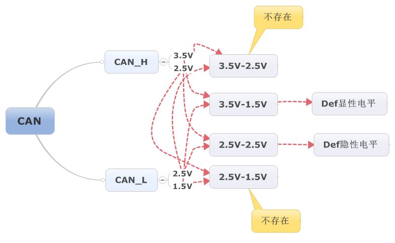
108. CAN bus (Controller Area Network). The CAN controller determines the bus level based on the potential difference on the two lines, which can be divided into dominant level and recessive level, one of which must be present.
109. The CAN bus has 6 characteristics: 1: multi-master control (all devices connected to the bus can become master devices, and the deviceID is used to determine device priority, with no concept of device address), 2: system is soft (there is no concept of device address), 3: communication speed is fast, communication distance is long (40M at 1Mbps, 10KM at 5kbps), 4: has error detection, error notification (notifying other devices) and error recovery function (forcing end of transmission and resending erroneous information), 5: fault confinement, when devices on the bus have continuous fault errors, the CAN controller will kick that controller out of the bus. 6: many connection nodes. In theory, it can be loaded indefinitely, but due to time delays and electrical loads, the actual number is limited. Reducing the transmission speed can appropriately increase the number of loadable devices.
110. The CAN protocol has two standards: ISO11898 (for high-speed rates of 125kbps~1Mbps) and ISO11519-2 (for low-speed rates below 125kbps)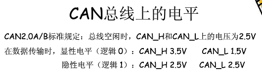
111.
112. The CAN protocol has five types of frames: data frame, remote frame, error frame, overload frame, and inter-frame. Among these, the first two frames have standard format (11-bit ID) and extended format (29-bit ID).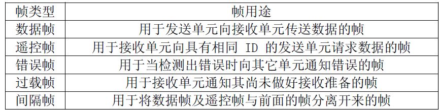
113. The composition of the data frame:
(1) Frame start. Indicates the start of the data segment.
(2) Arbitration segment. Indicates the priority of the frame.
(3) Control segment. Indicates the data byte and reserved bit segment.
(4) Data segment. The content of the data, a frame can send 0~8 bytes of data.
(5) CRC segment. Checks for transmission errors in the frame.
(6) ACK segment. Indicates normal reception acknowledgment.
(7) Frame end. Indicates the end of the data segment.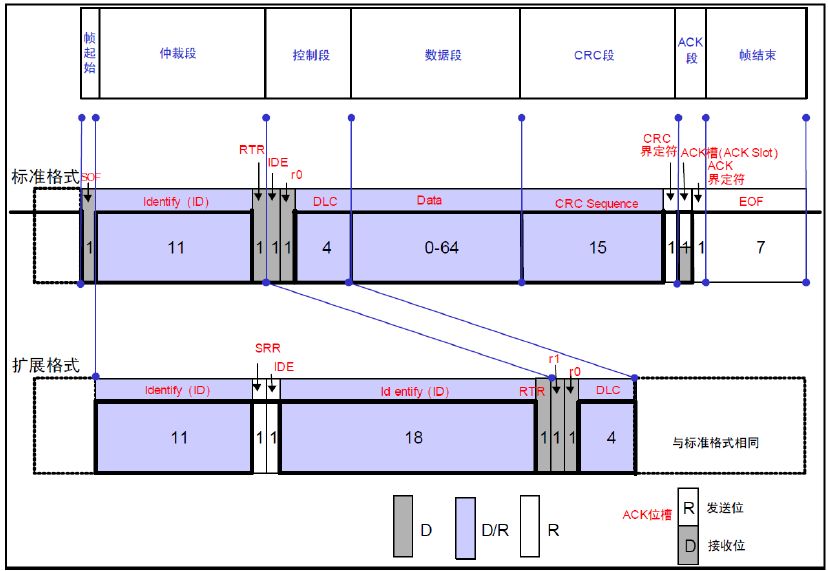
114. The STM32F103 series only has one CAN controller, with 3 sending mailboxes and a 2-level depth FIFO, and 14 filter groups.
115. Each filter group in STM32 can be configured as 1 32-bit filter and 2 16-bit filters. In addition, it can also be configured as mask mode (ID+ mask) and identifier list (ID and mask register are used asID register) mode.
116. Valid messages received by CAN are placed in the FIFO with a 3-level mailbox depth, which is entirely managed by hardware.
117. The baud rate of the CAN bus
118. Touch screens are generally divided into resistive touch screens and capacitive touch screens. The former detects the touch position using an A/D converter in the touch screen controller, obtaining X and Y coordinates after two A/D readings. Note: these X and Y values are relative to the touch screen, not the LCD screen. Therefore, two concepts must be noted: touch screen and LCD screen. These are two different concepts and two different physical structures, where the resistive touch screen consists of two conductive layers with a very thin transparent insulating layer sandwiched in between, while LCD refers to the display screen.
119. Resistive touch screens have X and Y, X and Y proportional factors, coordinate axis direction, and offsets. LCD also has its own parameters. The two are completely unrelated, so coordinate conversion is required during positioning. Formula: By calibrating the four points of the screen, a four-variable linear equation can be derived and solved.
120. The data frame format of the NEC protocol: synchronization code, address code, address inverse code, control code, control inverse code. The synchronization code consists of a 9ms low level and a 4.5ms high level, while the address code, address inverse code, control code, and control inverse code are all 8-bit data formats. Sent in the order of low bit first, high bit last.
121. When sending, the NEC protocol has a 560us 38KHz carrier signal, while when receiving, this part of the carrier signal is considered low level, while the remaining logical “1” and logical “0” times are considered high level.
122. Displacement within a unit time is defined as speed, which can be divided into linear speed and angular speed, corresponding to two types of sensors measuring these different speeds: linear speed sensors (accelerometers) and angular speed sensors (gyroscopes). The former is mostly used in static or slow-moving posture solutions, while the latter is mostly used in dynamic motion posture solutions.
123. According to standard conventions, zero acceleration (or zero G level) is typically defined as approximately half of the maximum output value (12-bit output is 4096, 10-bit output is 1024, etc.). For a 12-bit output accelerometer, zero G level equals 2048. Outputs greater than 2048 indicate positive acceleration. Outputs less than 2048 indicate negative acceleration. The quantity of acceleration is typically expressed in units of g (1g = 9.8m/s2 = gravitational acceleration). Acceleration can be calculated by determining the difference between the measured output and the zero G level, then dividing by the accelerometer’s sensitivity (expressed in counts/g or LSB/g). For a 2g accelerometer providing 12-bit digital output, the sensitivity is 819 counts/g or 819 LSB/g. Acceleration equals: a = (Aout – 2048)/(819 counts/g), in units of g.
124. The direction of acceleration measured by the accelerometer is opposite to the coordinate system set by the device because the principle states that when measuring force, a non-inertial reference frame is used, while the coordinate system studied in high school is an inertial reference frame. The former assumes a force acting on the object in the opposite direction of motion when the object accelerates; this force is the inertial force. The latter states that there is no inertial force, only inertia, since in the inertial coordinate system, we study the object, not the coordinate system (i.e., assuming the coordinate system is stationary relative to the Earth). When considering the coordinate system, when it moves, an inertial force f is generated, which acts on the object in the opposite direction of motion.
125. Thus, the essence of the accelerometer is to measure force rather than acceleration.
126. The NRF24L01 operates in the 2.4GHz band, and due to the higher frequency, it has a fast transmission rate of 2Mbps.
127. The FLASH module of STM32 consists of: main memory, information block, and flash memory interface register comprising three parts. The main memory is used to store code and const constants; the information block consists of two parts: boot program code and user-selected bytes. The boot program code is the built-in startup program from ST for serial downloading. Finally, the flash memory interface register is used to control operations on the flash area.
128. The CPU’s operating speed is much faster than FLASH’s operation speed; generally, the fastest FLASH access speed is ≤24MHz. If the CPU speed exceeds this frequency, a wait time (FLASH_ACR setting) must be added when reading FLASH.
129. When programming FLASH, writes must be half-words (16 bits). Moreover, the data in the area being written must be ensured to be 0xFFFF.
130. The STM32’s FSMC has HADDR[27:0], where [27:26] is used to select 4 different blocks in the BANK area. The remaining [25:0] connects to the address lines of the external storage area FSMC_A[25:0]. If the data width is 8 bits, then HADDR[25:0] corresponds directly to FSMC_A[25:0]. If the data width is 16 bits, then HADDR[25:1] corresponds to FSMC_A[24:0]. It is important to note: regardless of data width, the external FSMC_A[0] and A[0] always correspond.
131. The control of the LB and UB signals is handled automatically by hardware; when the AHB data width is smaller than the external memory’s data width, the LB and UB control signals are generated automatically (for example, byte read/write of 16-bit external memory).
132. __attribute__ (function attributes, variable attributes, type attributes, etc.). If using SRAM, you can use u32 sram_array[xx] __attribute__ ((at(0x68000000)) to allocate the entire external SRAM space to the variable sram_array, which has the property of being at address 0x68000000. Writing values into it directly writes to SRAM.
133. Memory management has a method called block memory management.
Note the allocation direction in the table, from top to bottom. Each item corresponds to a memory block. The values inside represent the status of the memory pool: if it is 0, it indicates that the memory has not been allocated; if non-zero, the size of the value indicates the number of continuously occupied memory blocks allocated to the pointer. For example, if the value is 20, it means that this item and the following 19 memory blocks have been continuously occupied and allocated to the pointer.
134. Classification of SD cards: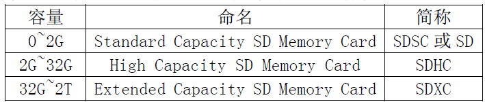
Generally, SD cards support two transmission modes: SD card mode (SDIO) and SPI mode. The former is a dedicated mode, thus faster in speed.
135. Common Chinese character encoding systems include GB2313, GB13000, GBK, and BIG5 (Traditional). Among them, GB2313 has only a few thousand Chinese characters, while GBK has over 20,000 characters.
136. To display Chinese characters, using a dot matrix format is not advisable, as it cannot look up Chinese characters. The method adopted is the encoding system. In the GBK standard, one Chinese character corresponds to 2 bytes: the former is called the area (0x81~0xFE), and the latter is (0x40~0x7E) and (0x80~0xFE). The former has 126 areas, and the latter has 190, so the total number of displayable Chinese characters is 126*190=23940 characters. Based on these two values, the character library can be referenced, which stores the dot matrix data for each character. This character library is very large; if the font is 16*16, then one font requires 32 bytes. Thus, the total space needed is 23940*32=748K, which is quite substantial, necessitating external FLASH to store this character library.
137. Due to the lack of international universality in the Chinese character encoding system, Unicode essentially includes almost all languages; thus, when operating Chinese characters in microcontrollers, the conversion between GBK and Unicode is necessary. Especially in FATFS, creating Chinese filenames and reading Chinese file information requires converting Unicode to GBK before modification operations, and then converting back to Unicode for saving. This means that the existence of both is due to the lack of standardization, and Unicode only contains 6064 Chinese characters, while GBK is evidently an extension of Chinese characters.
138. The encoding order of BMP images is from left to right, from bottom to top.
139. VS1053 is a high-performance digital audio decoding chip that decodes music audio files like mp3 from the SD card via SPI, outputting music to headphones. Headphone drivers can use TDA1308 chips, which are AB class headphone driver chips.
140.
141. IAP (In Application Programming) is a concept proposed for the convenience of later program updates. The specific implementation method is illustrated in the following image: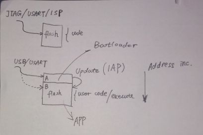
In ordinary programming, the code in FLASH is downloaded to the microcontroller using tools like JTAG and ISP. In IAP programming, FLASH is partitioned into A and B two areas, where area A is only allowed to download via USB/USART, serving as the code to update area B. Area B is the user’s code area, where the actual code is executed.
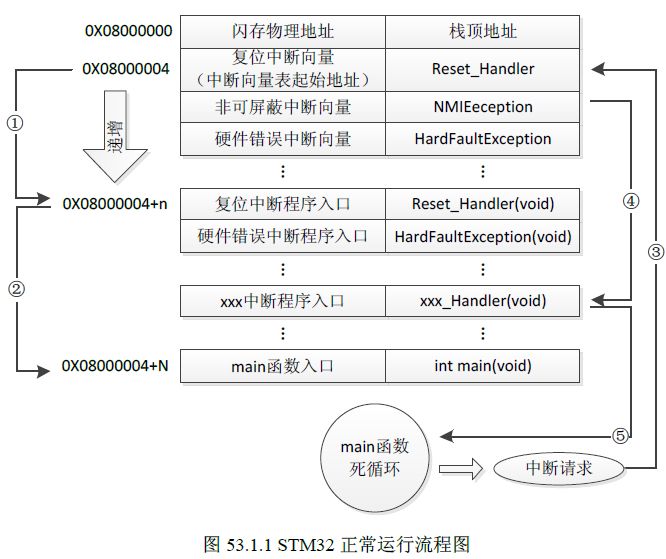
The above image shows the normal operation flow of STM32. After power-on reset, the system starts running the program at 0x80000004, where the reset interrupt vector is placed, then jumps to the reset interrupt program entry, and finally jumps to the main function to run the user program.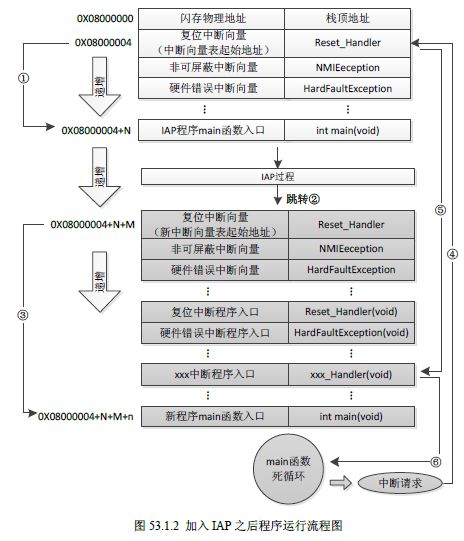
The above image illustrates the operation flow of STM32 after IAP is added. After power-on reset, it jumps to the main function of the IAP program to run the IAP process (this process is to burn the program code in the gray block into area B à code update). The subsequent process is the same as normal operation of STM32; if an interrupt request occurs, it still jumps to the interrupt vector table in area A, then jumps to the interrupt service entry in area B.
142. USB has four wires: VCC, GND, D+, D-. On the USB host, D+ and D- are both grounded through a 15K resistor, making both lines low level. In USB devices, high-speed devices connect D+ to VCC through a 1.5K resistor, while low-speed devices connect D- to VCC through a 1.5K resistor. This way, the host can detect the arrival of high levels on D+ and D- to identify whether a device is connected and recognize high-speed and low-speed devices.
143. UCOSII is a real-time operating system that is efficient, occupies little space (minimum kernel 2KB), has excellent implementation performance, strong scalability, and portability. 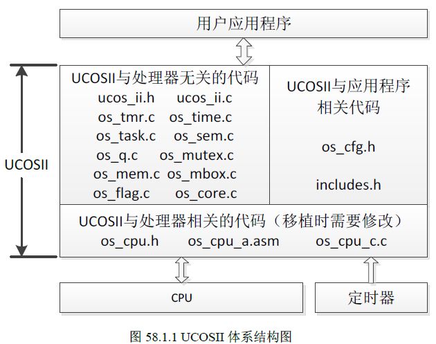 UCOS features multi-task concurrent operation (note that at any time only one task can occupy the CPU. Concurrency simply means tasks take turns occupying the CPU rather than working simultaneously.) It supports a maximum of 255 tasks concurrently.
This article is reprinted from the internet, and the copyright belongs to the original author. If you find it unsatisfactory, please contact us for deletion!
Advertisement
About Lichuang Mall
Lichuang Mall (WWW.SZLCSC.COM) was established in 2011, dedicated to providing customers with one-stop online procurement services for electronic components, with transaction volume leading the nation. The mall has over 10,000 square meters of modern component warehouses, with on-hand inventory exceeding 100,000 varieties. The group’s electronic full industry chain self-operated services include: online EDA (LCEDA) + industry-leading PCB prototyping/small batch + component mall + stencil manufacturing + SMT chip mounting + electronic design education and solutions. As a comprehensive, self-operated inventory, and quality-assured vertical mall for electronic components, all components from Lichuang Mall are procured from original manufacturers or authorized channels, ensuring genuine products and providing you with professional one-stop component procurement services.