1. Introduction to GPIO
GPIO stands for General-Purpose Input/Output, which can be simply understood as the pins controllable by STM32. The GPIO pins of the STM32 chip connect to external devices, enabling communication, control, and data acquisition with the outside world. The GPIO pins of the STM32 chip are divided into several groups, each with 16 pins, and all GPIO pins have basic input and output functionalities.
The most basic output function is controlled by the STM32, allowing the pin to output high and low levels, thus enabling switch control. For example, if the GPIO pin is connected to an LED, it can control the LED’s on/off state. If the pin is connected to a relay or transistor, it can control the on/off state of an external high-power circuit via the relay or transistor.
The most basic input function is to detect external levels. For instance, if the GPIO pin is connected to a button, it can distinguish whether the button is pressed based on the high or low level.
2. GPIO Block Diagram Analysis
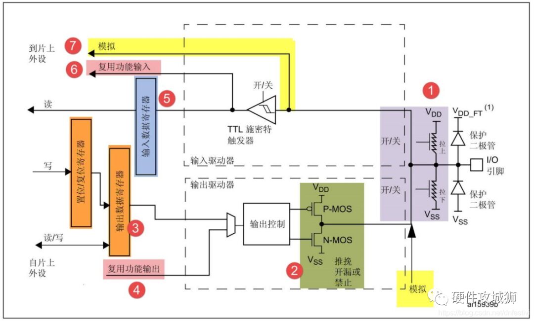
Through the GPIO hardware structure block diagram, we can gain an in-depth understanding of the GPIO peripherals and their various application modes. The diagram starts from the rightmost side, which represents the GPIO pins output from the STM32 chip, while the other components are located inside the chip.
1. Protection Diodes and Pull-up/Pull-down Resistors
The two protection diodes on the pin prevent excessive high or low voltage input from the external environment. When the pin voltage exceeds a certain level, the upper diode conducts, and when the pin voltage falls below Vss, the lower diode conducts, preventing abnormal voltages from damaging the chip.

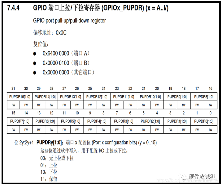
The pull-up and pull-down resistors allow us to control the default voltage state of the pin through their configurations. When the pull-up is enabled, the pin voltage is high; when the pull-down is enabled, the pin voltage is low. We can also set it to “neither pull-up nor pull-down mode,” which we call floating mode. In this mode, measuring the pin voltage with a voltmeter yields an uncertain value around 1.x volts. Therefore, generally, we choose to set the pin to either “pull-up mode” or “pull-down mode” to ensure a default state. The internal pull-up of STM32 is a “weak pull-up,” meaning the current output through the pull-up is very weak. For high current requirements, external pull-ups are necessary, controlled via the “Pull-up/Pull-down Register GPIOx_PUPDR” to manage the pin’s pull-up, pull-down, and floating modes.
2. P-MOS and N-MOS Transistors
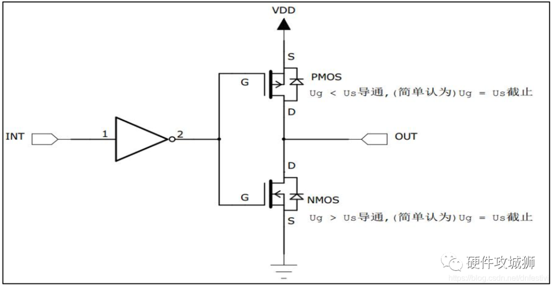
The GPIO pin circuit flows upwards to the “input mode” structure and downwards to the “output mode” structure after passing through the two protection diodes. Let’s first look at the output mode part, where the circuit comprises a unit circuit made of P-MOS and N-MOS transistors, allowing GPIO to have both “push-pull output” and “open-drain output” modes.
The so-called push-pull output mode is named based on the working principle of these two MOS transistors. In this structure, when a high level is input, the upper P-MOS conducts after inversion, while the lower N-MOS turns off, outputting a high level; conversely, when a low level is input, the N-MOS conducts after inversion, and the P-MOS turns off, outputting a low level. When switching between high and low levels, both transistors alternate conduction, with the P-MOS supplying current and the N-MOS pulling current, significantly enhancing load capacity and switching speed compared to ordinary methods. The low level of push-pull output is 0 volts, and the high level is 3.3V, as shown in the following equivalent circuit.
In the open-drain output mode, the upper P-MOS remains completely inactive. If we control the output to 0 (low level), the P-MOS turns off completely, and the N-MOS conducts, grounding the output. If we control the output to 1 (it cannot directly output a high level), both the P-MOS and N-MOS turn off, resulting in a high-impedance state where neither high nor low levels are output. To function normally, an external pull-up resistor must be connected, as shown in the equivalent circuit below. This configuration has a “wired AND” characteristic, meaning that if multiple open-drain mode pins are connected together, a high level is provided by the pull-up resistor only when all pins are in a high-impedance state. If one pin is low, the circuit effectively shorts to ground, making the entire line low (0 volts).
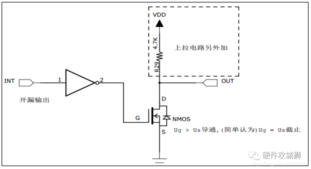
Push-pull output mode is generally used in scenarios requiring output levels of 0 and 3.3 volts with high-speed switching states. In STM32 applications, we typically use push-pull output mode unless open-drain mode is necessary. Open-drain output is commonly used in bus circuits like I2C and SMBUS that require “wired AND” functionality. Additionally, it is used in cases of voltage mismatch; for example, if a 5-volt high level is needed, a pull-up resistor can be connected externally with a 5-volt supply, configuring the GPIO to open-drain mode. When in high-impedance state, the pull-up resistor and power supply output 5 volts, as shown below.

3. Output Data Register
The input signal for the dual MOS transistor structure circuit mentioned earlier is provided by the GPIO “Output Data Register” GPIOx_ODR. Therefore, by modifying the value of the output data register, we can change the output level of the GPIO pin.
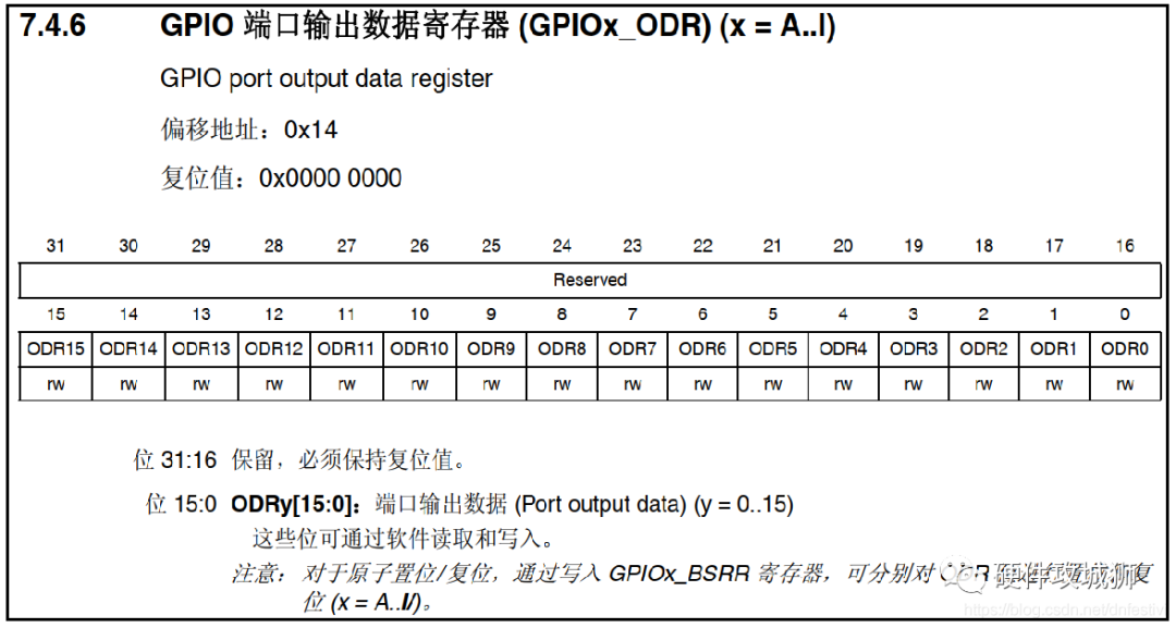
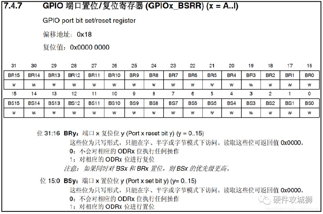
The “Set/Reset Register GPIOx_BSRR” can also influence the circuit’s output by modifying the output data register’s value.
4. Multiplexed Function Output
In the context of “multiplexed function output,” “multiplexing” refers to other on-chip peripherals of STM32 controlling GPIO pins. At this point, GPIO pins serve as part of that peripheral, representing a secondary function. The “multiplexed function output signals” from other peripherals are connected to the dual MOS transistor structure through a trapezoidal structure for switching selection.
For example, when using USART serial communication, a GPIO pin may be required as a transmission pin. At this time, the GPIO pin can be configured as a USART serial multiplexed function, allowing the peripheral to control the pin for data transmission.
5. Input Data Register
Looking at the upper half of the GPIO structure block diagram, it shows the GPIO pin’s connection after the pull-up and pull-down resistors, leading to the Schmitt trigger. The signal is converted from an analog signal to a digital signal of 0 or 1 after passing through the trigger, and then stored in the “Input Data Register GPIOx_IDR.” By reading this register, one can understand the GPIO pin’s level state.
6. Multiplexed Function Input
Similar to the “multiplexed function output” mode, in the “multiplexed function input” mode, the GPIO pin’s signal is transmitted to other on-chip peripherals of STM32, allowing that peripheral to read the pin’s state.
For instance, when using USART serial communication, a GPIO pin may be required as a reception pin. In this case, the GPIO pin can be configured as a USART serial multiplexed function, allowing USART to receive remote data through that communication pin.
7. Analog Input and Output
When a GPIO pin is used as an ADC input channel for voltage collection, it serves as an “analog input function.” In this case, the signal does not pass through the Schmitt trigger because the trigger only allows for two states (0 and 1). Thus, to capture the original analog signal, the signal source must be before the Schmitt trigger. Similarly, when the GPIO pin is used for DAC as an analog voltage output channel, it serves as an “analog output function,” where the DAC’s analog signal output does not pass through the dual MOS transistor structure. In the lower right corner of the GPIO structure block diagram, the analog signal directly outputs to the pin. Furthermore, when GPIO is used for analog functions (including input and output), the pull-up and pull-down resistors do not function. Even if pull-up or pull-down modes are configured in the register, they will not affect the analog signal’s input and output.
3. Summary of GPIO Operating Modes
1. Input Mode (Pull-up/Pull-down/Floating)
In input mode, the Schmitt trigger is enabled, and output is disabled. The data register updates every AHB1 clock cycle, and the I/O status can be read via the data register GPIOx_IDR. The AHB1 clock, by default, is generally 180MHz.
2. Output Mode (Push-pull/Open-drain, Pull-up/Pull-down)
In output mode, output is enabled. In push-pull mode, it operates in dual MOS transistor fashion, and the output data register GPIOx_ODR can control the I/O output high and low levels. In open-drain mode, only the N-MOS operates, and the output data register can control the I/O output high-impedance state or low level. The output speed can be configured to options of 2MHz, 25MHz, 50MHz, or 100MHz. The output speed indicates the highest switching frequency supported by the I/O for high and low levels. The higher the supported frequency, the greater the power consumption. If power consumption is not a strict requirement, the maximum speed can be set.
In this mode, the Schmitt trigger is enabled, allowing input. The actual state of the I/O can be read through the input data register GPIOx_IDR.
For output mode, pull-up, pull-down, or floating modes can be used. However, since in output mode, the pin level is influenced by the ODR register, with the ODR register corresponding to the pin’s bit being 0, the pin defaults to outputting a low level after initialization. Therefore, in this case, the pull-up can only slightly enhance the output current capacity but will not affect the pin’s default state.
3. Multiplexed Function (Push-pull/Open-drain, Pull-up/Pull-down)
In multiplexed function mode, output is enabled, and output speed can be configured. It can operate in open-drain and push-pull modes, but the output signal source comes from other peripherals, making the output data register GPIOx_ODR ineffective. Input is available, and the actual state of the I/O can be obtained through the input data register, but generally, the peripheral’s register is used to obtain this data signal.
In multiplexed function mode, pull-up, pull-down, or floating modes can be used. Similar to output mode, in this case, the pin defaults to outputting a low level after initialization, and the pull-up only slightly enhances the output current capacity but does not affect the pin’s default state.
4. Analog Input and Output
In analog input and output mode, the dual MOS transistor structure is disabled, the Schmitt trigger is inactive, and pull-up/pull-down are also disabled. Other peripherals conduct input and output via the analog channel.
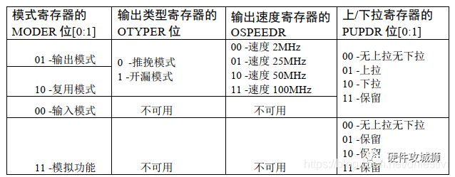
By writing different parameters to the GPIO registers, the GPIO’s operational mode can be changed. In GPIO peripherals, the “Mode Register GPIOx_MODER” can be configured to set GPIO to output/input/multiplexed/analog mode, the “Output Type Register GPIOx_OTYPER” configures push-pull/open-drain mode, the “Output Speed Register GPIOx_OSPEEDR” allows selection of output speeds of 2/25/50/100MHz, and the “Pull-up/Pull-down Register GPIOx_PUPDR” can configure pull-up/pull-down/floating modes. The specific parameters for each register are shown in the table below.