Main reference materials:
Bilibili @ Jiangxie Technology
STM32 Beginner’s Tutorial – 2023 Edition Detailed Explanation with Chinese Subtitles
Development material download link: https://pan.baidu.com/s/1h_UjuQKDX9IpP-U1Effbsw?pwd=dspb
Microcontroller kit: STM32F103C8T6 development board microcontroller C6T6 core board experimental board minimum system board kit
Article source file link: https://github.com/INKEM/Knowledge_Base
Introduction to SPI Peripherals
- • The STM32 integrates hardware SPI transceiver circuits, which can automatically perform clock generation, data transmission, and reception functions, reducing the burden on the CPU.
- • Configurable 8-bit/16-bit data frames, high-bit first/low-bit first
- • Clock frequency: derived from peripheral clock division
- • Supports multi-master model, master or slave operation (understanding)
- • Can be simplified to half-duplex/simplex communication (understanding)
- • Supports DMA
- • Compatible with I2S protocol (digital audio transmission protocol) (understanding)
- • STM32F103C8T6 hardware SPI resources: SPI1 (APB2), SPI2 (APB1)
SPI Block Diagram
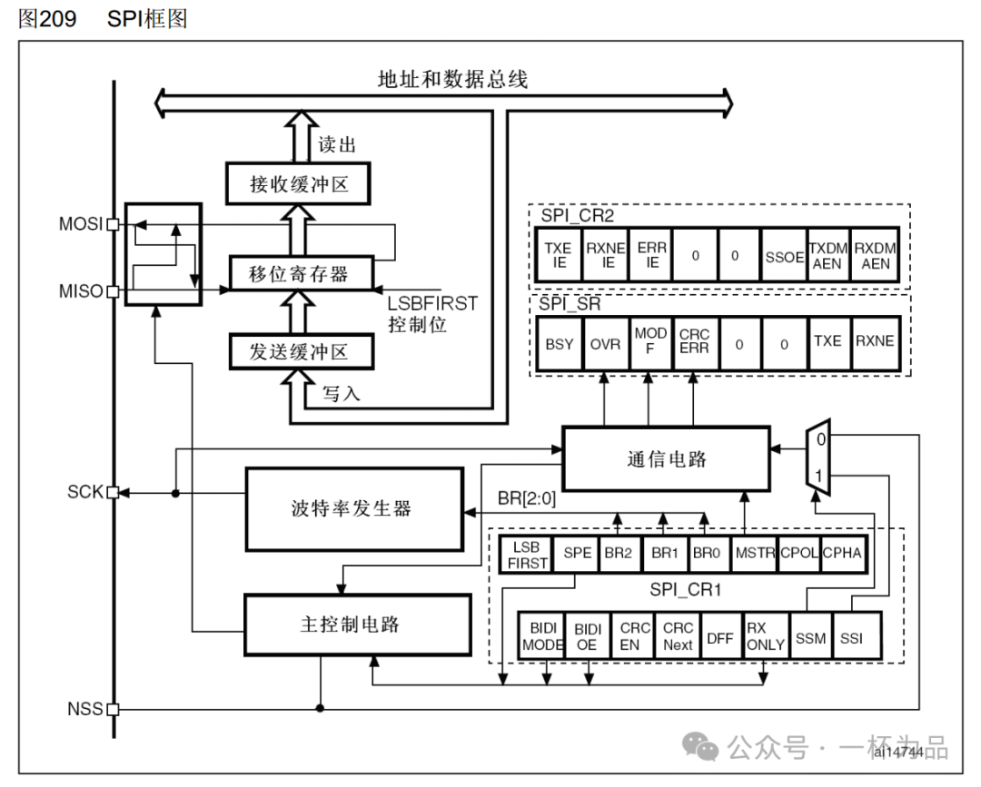
The upper left corner of the block diagram shows the data register and shift register working together for transmission and reception, similar to the design of UART and I2C, while the rest is the control circuit part. In the diagram, the data from the right end of the shift register is shifted out one bit at a time from MOSI, while the data from MISO is shifted in one bit at a time into the left end of the shift register. This is in low-bit first mode, and the LSBFIRST control bit can select low-bit first (write 1) or high-bit first (write 0). In high-bit first mode, data is output from the left end and input from the right end. The cross-connection of MOSI and MISO is used for pin swapping in master/slave mode, which is used when STM32 acts as a slave.
The send/receive buffer consists of the transmit data register (TDR) and receive data register (RDR), both occupying one DR address. When writing data, the data flows to TDR, and when reading data, it is read from RDR. The cooperation of the data register and shift register allows for continuous data flow. After the first data is written to TDR, when there is no data shifting in the shift register, the data in TDR will immediately transfer to the shift register to start shifting, setting the TXE bit in the status register. Following this, the next data can be written to TDR to wait for continuous transmission. The shift register automatically generates clock signals to shift out data while MISO data shifts in. Once the data shifting is complete, the data shifting in is also complete, and the shifted-in data will transfer as a whole from the shift register to RDR, setting the RXNE bit in the status register. At this point, the data in RDR must be read before the next data arrives to achieve continuous reception.
In the control circuit, the baud rate generator divides the peripheral clock to produce the SCK clock. For each clock generated, one bit is shifted in/out. The BR0~BR2 bits in SPI_CR1 control the division factor. LSBFIRST controls high-bit first/low-bit first, SPE is the SPI enable bit, MSTR configures master/slave mode, and CPOL and CPHA select one of the four SPI modes. Additionally, it is necessary to understand the last two bits TXE and RXNE mentioned in SPI_SR. SPI_CR2 includes interrupt/DMA enable bits, and NSS is used in multi-master mode, while the remaining parts of the block diagram are used less frequently.
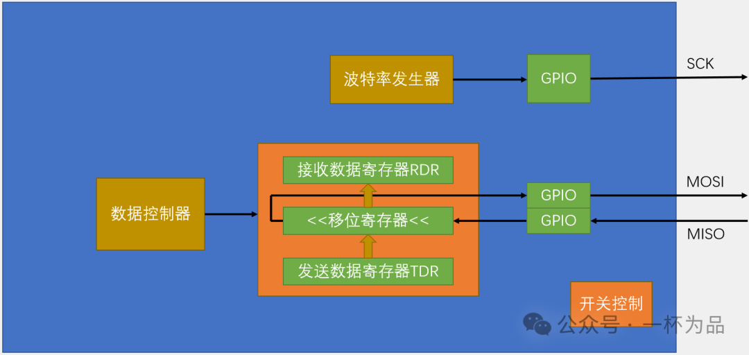
Basic Structure of SPI
Excluding unnecessary content, the SPI structure used in this experiment is as follows:
Timing Diagram
When reading and writing to DR, we focus on the timing diagrams for continuous and non-continuous transmission. Continuous transmission has higher performance but is more complex and less convenient to encapsulate; non-continuous transmission is easier to encapsulate and understand, making it simple to use. In practice, if there is no extreme pursuit of performance, non-continuous transmission is generally used. This experiment adopts non-continuous transmission.
Master Mode Full-Duplex Continuous Transmission
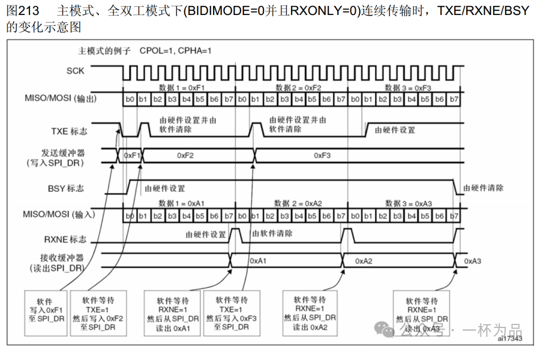
This example uses low-bit first, SPI mode 3, with SCK defaulting to high level, data shifting out on the falling edge and shifting in on the rising edge.
The input/output ends MISO/MOSI follow the clock changes to sequentially appear data bits. TXE is set by hardware when data is transferred from TDR to the shift register, and is cleared by software when new data is written to TDR. BSY is set by hardware during data transmission and cleared when idle. RXNE is set by hardware when data from the shift register is transferred to RDR, and is cleared by software when reading RDR. The continuous transmission process requires high software coordination; after each flag bit is generated, the data must be processed in a timely manner, allowing the clock to be generated continuously without any gaps between each byte transmission, achieving the highest transmission efficiency. The workflow can be summarized as writing data 1 → writing data 2 → reading data 1 → writing data 3 → reading data 2 → …, with the order of written and read data interleaved, making program design more complex.
Non-Continuous Transmission
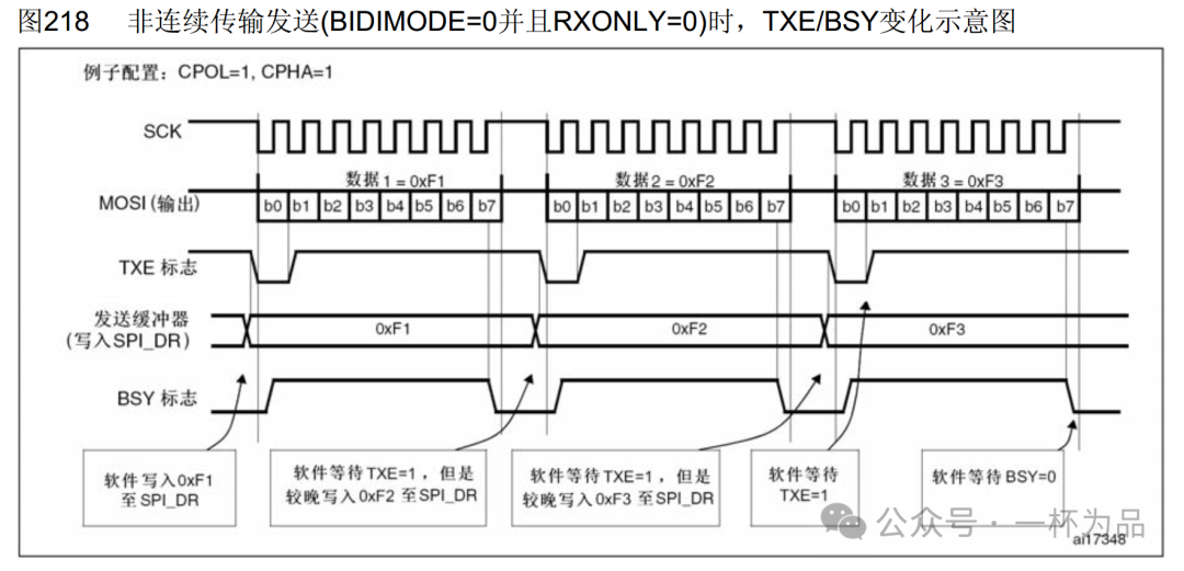
In non-continuous transmission, when TXE is set, we will wait for one byte’s timing to end, that is, after RXNE is set, first read the received data, and then write the next byte of data. This process will loop through the following four steps:
- 1. Wait for TXE=1
- 2. Write the data to be sent to TDR
- 3. Wait for RXNE=1
- 4. Read the data received from RDR
Function Details
Since the SPI peripheral is compatible with the I2S protocol, some function names are shared between the two.
SPI_I2S_DeInit Function
Overview: Restores default configuration.
Parameter: SPI name
SPI1/2/(3)SPI_Init Function
Overview: Initializes SPI.
Parameter one: SPI name
Parameter two: Pointer to SPI_InitTypeDef structure
SPI_InitTypeDef Structure
Member SPI_Mode: Master/Slave mode
SPI_Mode_Master/SlaveMember SPI_Direction: Pin configuration
SPI_Direction_2Lines_FullDuplex (full duplex with two lines) SPI_Direction_2Lines_RxOnly (two lines receive only) SPI_Direction_1Line_Rx (single line half-duplex receive) SPI_Direction_1Line_Tx (single line half-duplex transmit)Member SPI_DataSize: Data frame size
SPI_DataSize_16b/8b (16-bit/8-bit)Member SPI_FirstBit: High/Low bit first
SPI_FirstBit_MSB/LSB (high bit/low bit)Member SPI_BaudRatePrescaler: Baud rate prescaler
SPI_BaudRatePrescaler_2/4/8/16/32/64/128/256Member SPI_CPOL: Clock polarity (default level)
SPI_CPOL_Low/HighMember SPI_CPHA: Clock phase (sampling edge)
SPI_CPHA_1/2Edge (first/second edge)Member SPI_NSS: NSS mode
SPI_NSS_Soft/High (software/hardware)Member SPI_CRCPolynomial: CRC check polynomial, default is 7
SPI_StructInit Function
Overview: Initializes SPI_InitTypeDef structure.
Parameter: Pointer to SPI_InitTypeDef structure
SPI_Cmd Function
Overview: Enables SPI.
Parameter one: SPI name
Parameter two: Enable/Disable
SPI_I2S_ITConfig Function
Overview: Enables SPI interrupts.
Parameter one: SPI name
Parameter two: SPI interrupt
SPI_I2S_IT_TXE/RXNE/ERRParameter three: Enable/Disable
SPI_I2S_DMACmd Function
Overview: Enables DMA.
Parameter one: SPI name
Parameter two: DMA request
SPI_I2S_DMAReq_Tx/RxParameter three: Enable/Disable
SPI_I2S_SendData Function
Overview: Writes data to DR.
Parameter one: SPI name
Parameter two: Data
SPI_I2S_ReceiveData Function
Overview: Reads data from DR.
Parameter: SPI name
Interrupt Flag Functions
SPI_GetFlagStatus Function
SPI_ClearFlag Function
Parameter one: SPI name
Parameter two: SPI flag
SPI_I2S_FLAG_TXE SPI_I2S_FLAG_RXNE Other flags not currently usedSPI_GetITStatus Function
SPI_ClearITPendingBit Function
Parameter one: SPI name
Parameter two: SPI interrupt
Experiment 27 Hardware SPI Read/Write W25Q64
This experiment modifies the MySPI.c program to use hardware logic for all pins except the SS pin based on software SPI.
MySPI.c
#include "stm32f10x.h"

// SS pin is still retained for software simulation
void MySPI_W_SS(uint8_t BitValue)
{
    GPIO_WriteBit(GPIOA, GPIO_Pin_4, (BitAction)BitValue);
}

// Other pins are changed to hardware implementation
void MySPI_Init(void)
{
    RCC_APB2PeriphClockCmd(RCC_APB2Periph_GPIOA, ENABLE);
    // Enable SPI peripheral clock
    RCC_APB2PeriphClockCmd(RCC_APB2Periph_SPI1, ENABLE);

    // SS pin remains as general push-pull output
    GPIO_InitTypeDef GPIO_InitStructure;
    GPIO_InitStructure.GPIO_Mode = GPIO_Mode_Out_PP;
    GPIO_InitStructure.GPIO_Pin = GPIO_Pin_4;
    GPIO_InitStructure.GPIO_Speed = GPIO_Speed_50MHz;
    GPIO_Init(GPIOA, &GPIO_InitStructure);
    // MOSI/SCK pins changed to alternate function push-pull output
    GPIO_InitStructure.GPIO_Mode = GPIO_Mode_AF_PP;
    GPIO_InitStructure.GPIO_Pin = GPIO_Pin_5 | GPIO_Pin_7;
    GPIO_Init(GPIOA, &GPIO_InitStructure);
    // MISO remains as pull-up input
    GPIO_InitStructure.GPIO_Mode = GPIO_Mode_IPU;
    GPIO_InitStructure.GPIO_Pin = GPIO_Pin_6;
    GPIO_Init(GPIOA, &GPIO_InitStructure);

    SPI_InitTypeDef SPI_InitStructure;
    SPI_InitStructure.SPI_Mode = SPI_Mode_Master;
    SPI_InitStructure.SPI_Direction = SPI_Direction_2Lines_FullDuplex;
    SPI_InitStructure.SPI_DataSize = SPI_DataSize_8b;
    SPI_InitStructure.SPI_FirstBit = SPI_FirstBit_MSB;
    SPI_InitStructure.SPI_BaudRatePrescaler = SPI_BaudRatePrescaler_128;
    SPI_InitStructure.SPI_CPHA = SPI_CPHA_1Edge;
    SPI_InitStructure.SPI_CPOL = SPI_CPOL_Low;
    SPI_InitStructure.SPI_CRCPolynomial = 7;
    // NSS pin is not used, choose software NSS
    SPI_InitStructure.SPI_NSS = SPI_NSS_Soft;
    SPI_Init(SPI1, &SPI_InitStructure);
    // Enable SPI peripheral
    SPI_Cmd(SPI1, ENABLE);

    MySPI_W_SS(1);
}

void MySPI_Start(void)
{
    MySPI_W_SS(0);
}

void MySPI_Stop(void)
{
    MySPI_W_SS(1);
}

uint8_t MySPI_SwapByte(uint8_t ByteSend)
{
    // Wait for TXE
    while(!SPI_I2S_GetFlagStatus(SPI1, SPI_I2S_FLAG_TXE));
    // Write to DR
    SPI_I2S_SendData(SPI1, ByteSend);
    // Wait for RXNE
    while(!SPI_I2S_GetFlagStatus(SPI1, SPI_I2S_FLAG_RXNE));
    // Read from DR
    return SPI_I2S_ReceiveData(SPI1);
}