Click the blue text above to follow us
Embedded Training – Choose Jufeng Smart Link
1. Overview
In the previous chapter “STM32 – Mastering SPI Principles (Part I)”, I explained some of the underlying architecture of SPI. In this article, we will demonstrate how to use the SPI principles to write data to the W25Q64 chip and print the corresponding content via the serial port. This article will focus more on the application, and you can simply use the underlying functions without needing to write the corresponding code in the SPI.c file independently.
2. Introduction to W25Q64
Introduction
The W25Q64 is a serial SPI Flash memory produced by Winbond, officially named W25Q64JV, where “64” indicates its capacity of 64 Mbit = 8MB. It uses the SPI communication protocol and is suitable for embedded systems that require large-capacity non-volatile storage. Flash memory is non-volatile, meaning data is not lost when power is removed, and it can be erased and rewritten multiple times, although its lifespan is limited. Examples include:
IoT devices, data loggers, audio/image caching, configuration file storage, etc.
Hardware Appearance
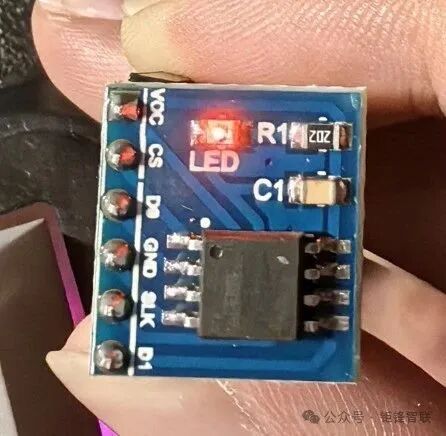
Main Features
| Feature Item | Description |
|---|---|
| Interface Protocol | SPI (supports up to 104MHz) |
| Operating Voltage | 2.7V ~ 3.6V (so be sure to connect to 3.3V in subsequent wiring) |
| Capacity | 64 Mbit (= 8MB) |
| Minimum Writable Unit | Page = 256 bytes |
| Minimum Erasable Unit | Sector = 4KB |
| Larger Erasable Unit | Block = 64KB or 32KB |
| Erase Entire Chip | Supported |
| ID Read | Supports reading manufacturer ID and device ID |
| Status Register | Three (SR1, SR2, SR3) |
When writing data, we usually write in “pages” and erase in “sectors” or “blocks”. In this article, we will use “sectors” for erasure.
Common SPI Commands
| Command Name | Command Code | Function |
|---|---|---|
| Write Enable | <span>0x06</span> |
Enable writing |
| Page Program | <span>0x02</span> |
Page write (up to 256 bytes) |
| Read Data | <span>0x03</span> |
Read data |
| Sector Erase | <span>0x20</span> |
Erase 4KB sector |
| Block Erase | <span>0xD8</span> |
Erase 64KB block |
| Chip Erase | <span>0xC7</span> |
Erase entire chip |
| Read Status Register | <span>0x05</span> |
Read status register 1 (to check if busy) |
| Manufacturer/Device ID | <span>0x90</span> |
Read chip ID |
We will explain the code later, and there are many commands; just remember a few, and if needed, refer to the W25Q64 chip manual.
3. Code Section
Introduction
Before we dive into the code, we need to establish the hardware connections.
| W25Q64 Pin | Name | Function Description | STM32 Connection Pin (SPI1) |
|---|---|---|---|
| 1 | CS | Chip Select (active low) | PA4 |
| 2 | DO | Data Output (MISO) | PA6 |
| 3 | GND | Ground | GND |
| 4 | DI | Data Input (MOSI) | PA7 |
| 5 | CLK | Serial Clock | PA5 |
| 6 | VCC | Power Supply | 3.3V |
SPI.c
void W25Q64_SPI_Init(void){
    GPIO_InitTypeDef GPIO_InitStructure;    SPI_InitTypeDef SPI_InitStructure;
    RCC_APB2PeriphClockCmd(RCC_APB2Periph_GPIOA | RCC_APB2Periph_SPI1, ENABLE);
    // CS pin (PA4)    GPIO_InitStructure.GPIO_Pin = GPIO_Pin_4;    GPIO_InitStructure.GPIO_Mode = GPIO_Mode_Out_PP;    GPIO_InitStructure.GPIO_Speed = GPIO_Speed_50MHz;    GPIO_Init(GPIOA, &GPIO_InitStructure);    GPIO_SetBits(GPIOA, GPIO_Pin_4);  // Pull CS high
    // SCK (PA5), MOSI (PA7)    GPIO_InitStructure.GPIO_Pin = GPIO_Pin_5 | GPIO_Pin_7;    GPIO_InitStructure.GPIO_Mode = GPIO_Mode_AF_PP;    GPIO_Init(GPIOA, &GPIO_InitStructure);/*      Why configure CS as push-pull output while SCK and MOSI as alternate function push-pull?      Answer: These pins (like PA5, PA7) are controlled by the SPI1 peripheral.      You cannot control them with GPIO_SetBits/GPIO_ResetBits, but through SPI_SendData.      As for CS, it acts as a normal IO pin.*/
    // MISO (PA6)    GPIO_InitStructure.GPIO_Pin = GPIO_Pin_6;    GPIO_InitStructure.GPIO_Mode = GPIO_Mode_IN_FLOATING;    GPIO_Init(GPIOA, &GPIO_InitStructure);
    // SPI Configuration    SPI_InitStructure.SPI_Direction = SPI_Direction_2Lines_FullDuplex;    SPI_InitStructure.SPI_Mode = SPI_Mode_Master;    SPI_InitStructure.SPI_DataSize = SPI_DataSize_8b;    SPI_InitStructure.SPI_CPOL = SPI_CPOL_Low;        // CPOL=0, idle low    SPI_InitStructure.SPI_CPHA = SPI_CPHA_1Edge;    // CPHA=0, sample on first edge    SPI_InitStructure.SPI_NSS = SPI_NSS_Soft;    SPI_InitStructure.SPI_BaudRatePrescaler = SPI_BaudRatePrescaler_256;    SPI_InitStructure.SPI_FirstBit = SPI_FirstBit_MSB;    SPI_InitStructure.SPI_CRCPolynomial = 7;    SPI_Init(SPI1, &SPI_InitStructure);
    SPI_Cmd(SPI1, ENABLE);
}
// Send/Receive a byte
uint8_t w25q64_spi_swap_byte(uint8_t data){
    // TXE is 1 indicates data can be written
    while(SPI_I2S_GetFlagStatus(SPI1, SPI_I2S_FLAG_TXE) == RESET);
    SPI_I2S_SendData(SPI1, data); // RXNE is 1 indicates data has been received, can be read
    while(SPI_I2S_GetFlagStatus(SPI1, SPI_I2S_FLAG_RXNE) == RESET);
    // Return the data read from SPI1
    return SPI_I2S_ReceiveData(SPI1);
}
The above code has already been written in the previous article “STM32 – Mastering SPI Principles (Part I)”. If you do not understand the above code, please refer to the previous article. Next, we will explain other codes.
New Code Part One:
void W25Q64_CS_LOW(void) { GPIO_ResetBits(GPIOA, GPIO_Pin_4); }
void W25Q64_CS_HIGH(void) { GPIO_SetBits(GPIOA, GPIO_Pin_4); }
Since SPI communication requires the chip select signal to be pulled low before data communication, to disable SPI communication, pull the chip select high.
New Code Part Two:
void W25Q64_WriteEnable(void){
    W25Q64_CS_LOW();
    w25q64_spi_swap_byte(0x06);  // Write enable command
    W25Q64_CS_HIGH();
}
Send the 0x06 command to put the Flash into “write enable” state (a necessary prerequisite).
uint8_t W25Q64_ReadSR1(void){
    uint8_t status;
    W25Q64_CS_LOW();
w25q64_spi_swap_byte(0x05);/*
    Send command 0x05 to the W25Q64 chip, indicating that I want to read status register 1.
    Sending 0x05 via SPI is the fixed "read status register 1" command for W25Q64.
    The purpose is to check if busy.*/
    status = w25q64_spi_swap_byte(0xFF);/*
    This step is "actually for receiving"; it doesn't matter what is sent, 0xFF is just a placeholder.
    This is because the essence of the SPI protocol is "full-duplex synchronous communication".
    Therefore, when receiving data, you must also "send" a byte, otherwise the SPI clock will not run, and the slave will not send data.
*/
    W25Q64_CS_HIGH();
    return status;
}
This function reads status register 1 to determine the current status of the Flash, commonly used to check if it is busy (BSY bit). The contents of status register 1 (SR1) in W25Q64 are as follows:
| Bit Number | Name | Description |
|---|---|---|
| Bit7 | SRP | Status Register Protection Bit |
| Bit6 | SEC | Sector Protection Indicator |
| Bit5 | TB | Top/Bottom Protection Area Select Bit |
| Bit4 | BP2 | Block Protection Bit 2 |
| Bit3 | BP1 | Block Protection Bit 1 |
| Bit2 | BP0 | Block Protection Bit 0 |
| Bit1 | WEL | Write Enable Latch |
| Bit0 | BUSY | Flash Busy Flag (1 = programming/erasing, 0 = idle) |
To check if the Flash is busy, we only need to look at Bit0. If it is busy, SPI communication is not allowed; if it is not busy, communication can proceed.
New Code Part Three:
void W25Q64_WaitBusy(void){
    while((W25Q64_ReadSR1() & 0x01) == 0x01); // Here we use & (bitwise AND), not && (logical AND)
}
Here is a brief summary of the difference between & and &&:
| Operator | Name | Used For | Example |
|---|---|---|---|
<span>&</span> |
Bitwise AND | Compares the binary bits of two numbers bit by bit | <span>0x05 & 0x01</span> → <span>0x01</span> |
<span>&&</span> |
Logical AND | Used to check if both conditions are true | <span>a && b</span> → If both are non-zero, it is true |
In this case, we only need to check if Bit0 is 1. If it is 1, the function W25Q64_WaitBusy will block, and execution will not proceed. If it is 0, it indicates idle.
New Code Part Four:
void W25Q64_SendAddress(uint32_t addr){
    w25q64_spi_swap_byte((addr >> 16) & 0xFF);
    w25q64_spi_swap_byte((addr >> 8) & 0xFF);
    w25q64_spi_swap_byte(addr & 0xFF);/*
    Split a 24-bit address into 3 bytes, sending from high to low via SPI to the Flash chip, which is a prerequisite for read, write, and erase operations.
*/
}
New Code Part Five (Read):
void W25Q64_ReadData(uint32_t addr, uint8_t* buf, uint32_t size){
    uint32_t i;
    W25Q64_CS_LOW();
    w25q64_spi_swap_byte(0x03);
    W25Q64_SendAddress(addr);
    for(i = 0; i < size; i++)
        buf[i] = w25q64_spi_swap_byte(0xFF);
    W25Q64_CS_HIGH();
}
Why do we send 0x03 (read data command) first here, instead of sending the address like in I2C? This is the unique aspect of SPI. To illustrate, consider this analogy: when you go to a library to borrow a book, the process is as follows:
You say: “I want to read a book” — this step is like w25q64_spi_swap_byte(0x03); sending the read command.
The library responds: “Which book do you want?” — you then provide the address: 0x000123.
Only then does the library fetch the data for you — this begins the data reading phase.
This is because SPI is “streaming command-based communication”, unlike I2C, which has the concept of “device address + internal register address”. The W25Q64 is an SPI Flash, and it specifies:
To read data, you must first send a read command (0x03),then tell me the address so I know where to read from.
New Code Part Six (Write):
void W25Q64_WritePage(uint32_t addr, uint8_t* data, uint16_t size){
    uint16_t i;
    W25Q64_WriteEnable();
    W25Q64_CS_LOW();
    w25q64_spi_swap_byte(0x02);
    W25Q64_SendAddress(addr);
    for(i = 0; i < size; i++)
        w25q64_spi_swap_byte(data[i]);
    W25Q64_CS_HIGH();
    W25Q64_WaitBusy();
}
If you observe carefully, you will notice that writing has two additional functions: W25Q64_WriteEnable() and W25Q64_WaitBusy(). This is because all operations that modify data (write/erase) in W25Q64 must go through “write enable” authorization and wait for the chip to complete the operation; reading operations are non-destructive, so these prerequisites are not needed.
New Code Part Seven (Erase):
void W25Q64_EraseSector(uint32_t addr){
    W25Q64_WriteEnable();
    W25Q64_WaitBusy();
    W25Q64_CS_LOW();
    w25q64_spi_swap_byte(0x20);
    W25Q64_SendAddress(addr);
    W25Q64_CS_HIGH();
    W25Q64_WaitBusy();
}
Erase a 4KB area in Flash by “sector”.
New Code Part Eight (Get Address ID):
uint16_t W25Q64_ReadID(void){
    uint16_t device_id = 0;
    W25Q64_CS_LOW();
    w25q64_spi_swap_byte(0x90);
    w25q64_spi_swap_byte(0x00);
    w25q64_spi_swap_byte(0x00);
    w25q64_spi_swap_byte(0x00);
    device_id = w25q64_spi_swap_byte(0xFF) << 8;
    device_id |= w25q64_spi_swap_byte(0xFF);
    W25Q64_CS_HIGH();
    return device_id;
}
This function retrieves the manufacturer ID and device ID of the chip, which is not mandatory to use; it can be used selectively.
main.c
#include "stm32f10x.h"
#include "spi.h"
#include "usart.h"
uint8_t tx_data[16] = "Hello STM32!";
uint8_t rx_data[16] = {0};
int main(void){
    my_usart_Config();       // Serial port initialization
    W25Q64_SPI_Init();       // SPI initialization
    printf("Start test...\r\n");
    uint16_t id = W25Q64_ReadID();    printf("Flash ID = 0x%04X\r\n", id);
    if(id == 0xEF16)  // W25Q64 normal ID; w25q128 ID is 0xEF17    {
        printf("W25Q64 detected.\r\n");
        // Erase sector
        W25Q64_EraseSector(0x000000);
        printf("Sector erased.\r\n");
        // Write a page, sizeof(rx_data) indicates how many bytes to read
        W25Q64_WritePage(0x000000, tx_data, sizeof(tx_data));
        printf("Page written.\r\n");
        // Read data
        W25Q64_ReadData(0x000000, rx_data, sizeof(rx_data));
        // Print the read data
        printf("Read data: %s\r\n", rx_data);
    }    else    {
        printf("W25Q64 not found.\r\n");
    }
    while(1);
}
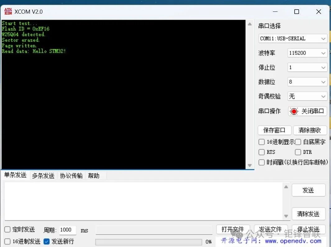
As shown above, I printed the contents of the W25Q64 via the serial port. Of course, I will explain it clearly to you. The first page is 0x000000, but what about the second page? If I want to write to another page, what should I do?
| Page Number | Starting Address (Hex) | Range |
|---|---|---|
| Page 0 | <span>0x000000</span> |
0x000000 ~ 0x0000FF |
| Page 1 | <span>0x000100</span> |
0x000100 ~ 0x0001FF |
| Page 2 | <span>0x000200</span> |
0x000200 ~ 0x0002FF |
| Page 3 | <span>0x000300</span> |
0x000300 ~ 0x0003FF |
| … | … | … |
| Page 255 | <span>0x00FF00</span> |
0x00FF00 ~ 0x00FFFF |
| Page 256 | <span>0x010000</span> |
0x010000 ~ 0x0100FF |
| … | … | … |
So, if we want to write to another page, you understand, right? We just need to change the values of the first four positions.
For example, if you want to write to Page 3, set the address to 3 × 256 = 0x000300.
If you want to write to Page 10? Then it would be 10 × 256 = 0x000A00.
In summary: Page Number × 256 = Starting Address to Write.
Let me add: The normal ID for W25Q64 is 0xEF16; the ID for w25q128 is 0xEF17.
4. Results

Original link: https://blog.csdn.net/2301_81650162/article/details/149122053