
1. Introduction
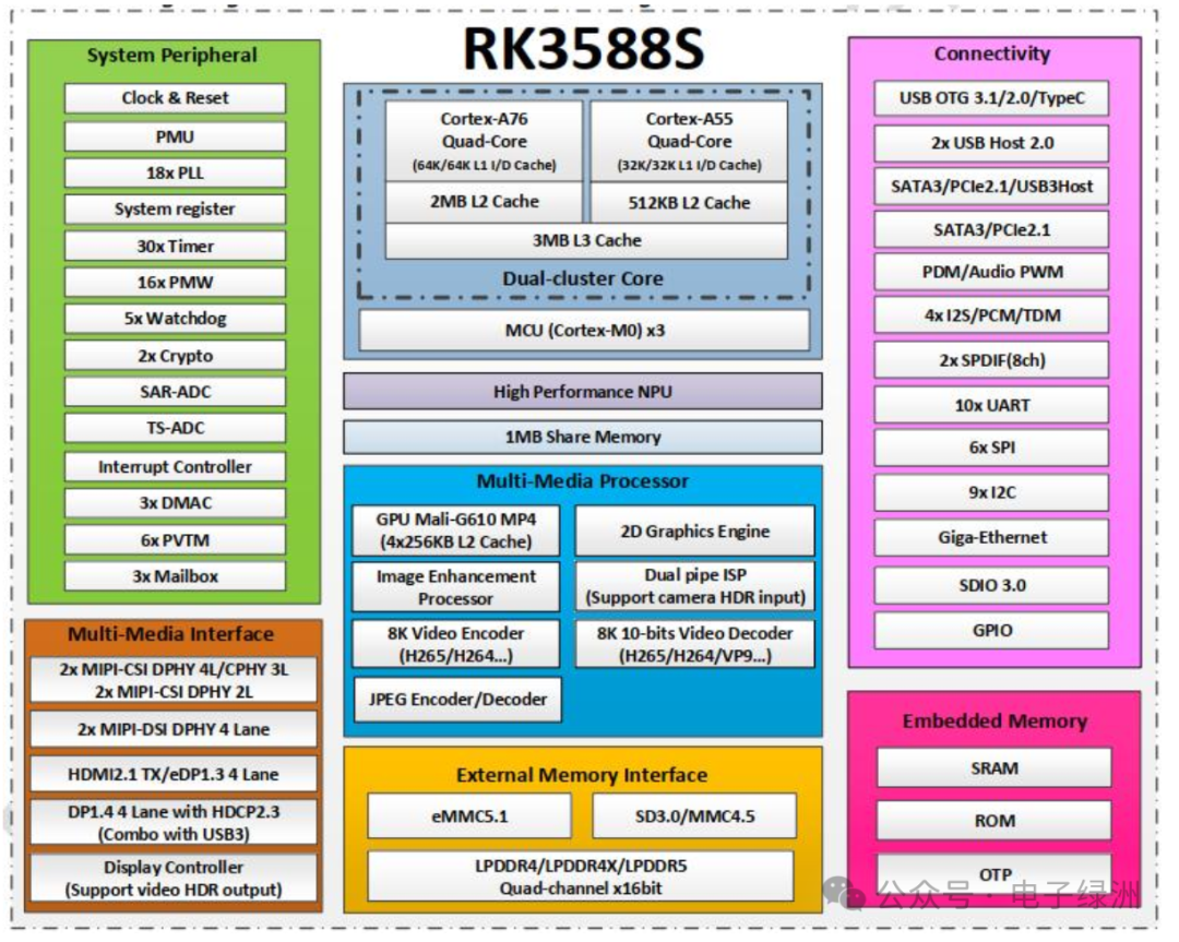
The RK3588S is a high-performance, low-power application processor chip, featuring four Cortex-A76 and four Cortex-A55 cores along with an independent NEON coprocessor, suitable for tablets, VR, personal mobile internet devices, and other multimedia products.
The RK3588S integrates various powerful embedded hardware engines, providing excellent performance for high-end applications, supporting 8K@60fps H.265 and VP9 decoders, 8K@30fps H.264 decoder, and 4K@60fps AV1 decoder; it also supports 8K@30fps H.264 and H.265 encoders, high-quality JPEG encoder/decoder, dedicated image pre-processor, and post-processor.
It features a built-in 3D GPU that is fully compatible with OpenGL ES1.1/2.0/3.2, OpenCL 2.2
and Vulkan 1.2.
A special 2D hardware engine with an MMU maximizes display performance and provides a smooth operating experience.
A next-generation fully hardware-based ISP (Image Signal Processor) with a maximum of 48M pixels is introduced, implementing many algorithm accelerators such as HDR, 3A, LSC, 3DNR, 2DNR, sharpening, dehazing, fisheye correction, and gamma correction.
The embedded NPU supports INT4, INT8, INT16, and FP16 mixed operations, with a computing power of up to 6 TOPS.
The RK3588S features a high-performance 4-channel external memory interface capable of supporting systems with high memory bandwidth requirements, and provides a complete set of peripheral interfaces to flexibly support various applications.
The RK3588S is manufactured using a 8nm process technology.
Chip Block Diagram:
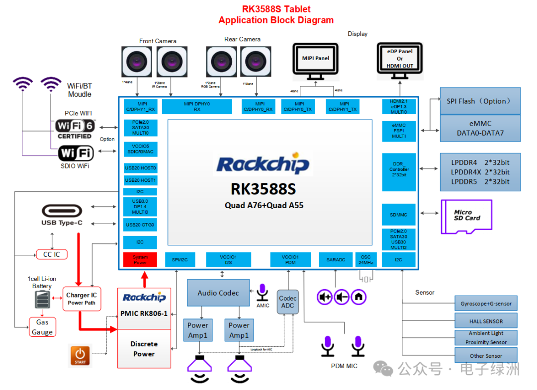
RK3588S Tablet (1 Cell) Block Diagram:
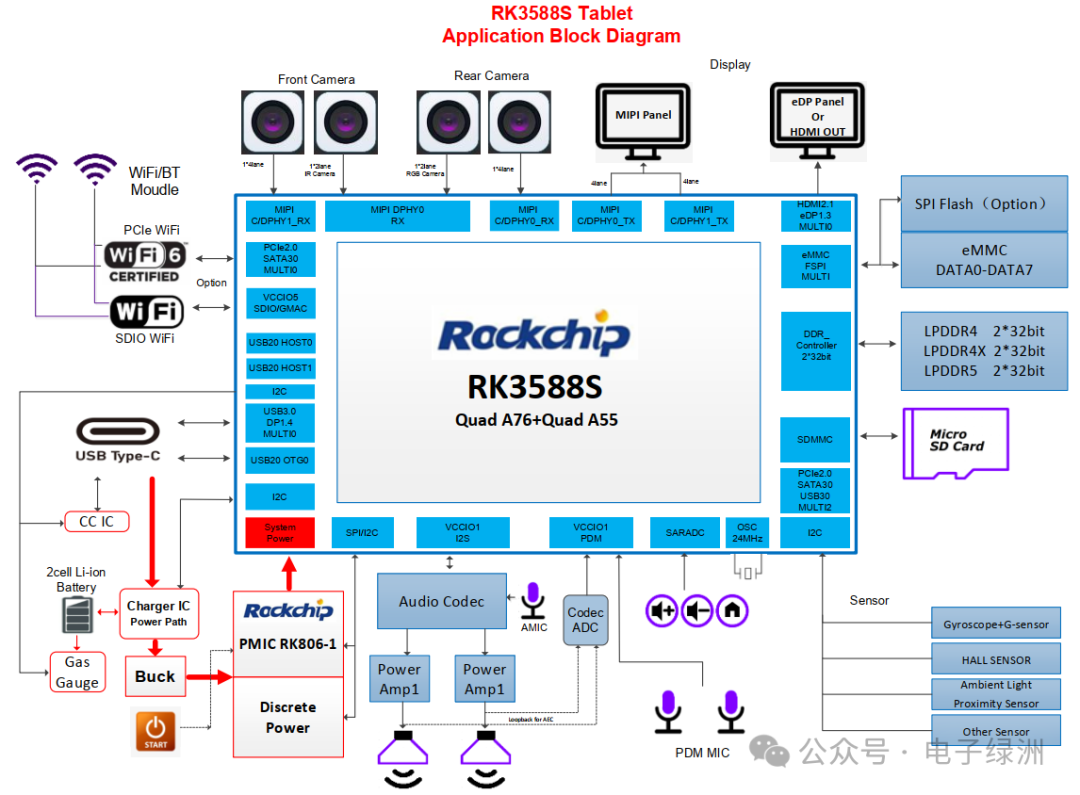
RK3588S Tablet (2 Cells) Block Diagram:
2. Reset
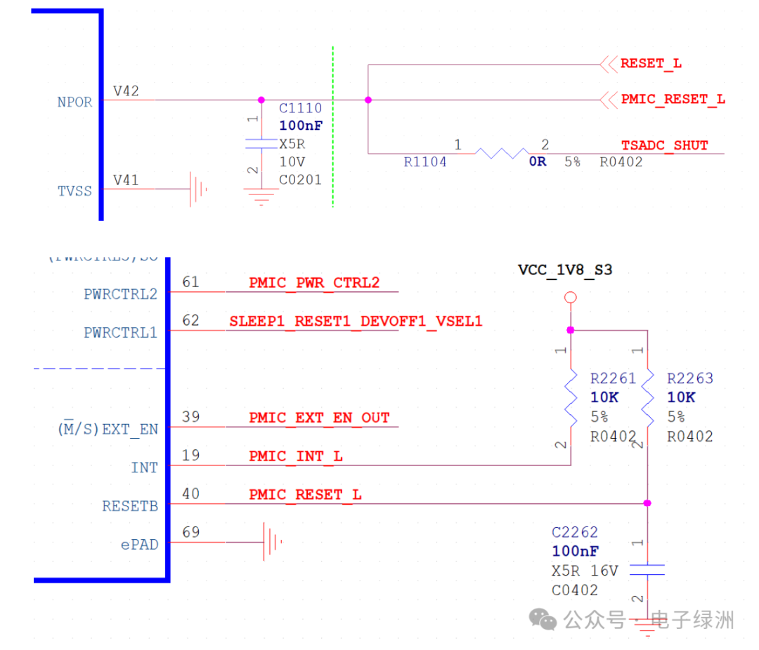
The hardware reset of the RK3588S chip is input through the Pin V42 (NPOR) pin, which must be controlled externally and is active low. To ensure the chip’s stability and normal operation, the minimum reset time required is 100 cycles of the 24MHz main clock (1/24MHz, 0.04uS), which is at least 4us.
The Pin V42 (NPOR) pin requires a 100nF capacitor to eliminate jitter on the reset signal, enhance anti-interference capability, and prevent abnormal resets caused by false triggers.
The pull-up power supply for the RESET_L network must be consistent with the IO power domain of the NPOR pin (PMUIO1_1V8).
In the PCB design of the reset circuit, please note:
A. When laying out, the RESETn reset signal should be kept away from the board edge and metal connectors to prevent abnormal resets caused by ESD;
B. The filtering capacitor for RESETn should be placed as close to the chip pin as possible, with the signal passing through the capacitor before entering the chip. Note that the ground pad of the filtering capacitor must have a 0402 ground via, and if space allows, it is recommended to add more than two for better grounding;
C. The RESETn signal should be kept away from strong interference signals such as DCDC and RF to prevent interference. If the trace is long, it is recommended to use ground wrapping, and add at least one GND via every 400 mil;
D. The TVS protection diode for the RESETn button should be placed as close to the button as possible, with the signal topology as follows: button —> TVS —> 100 ohm —> capacitor (near CPU & PMIC) —> CPU & PMIC; in the event of ESD, the ESD current must first pass through the TVS device for attenuation.
3. Watchdog
The RK3588S chip integrates a Watchdog Timer, which can output a low level through the TSADC_SHUT pin to perform a hardware reset on the RK3588S when a reset signal is generated.
The watchdog is a hardware timer used to automatically reset the system in case of failure, preventing deadlocks, enhancing reliability, and assisting in debugging. By counting time and performing “dog feeding” operations, the watchdog can effectively improve the stability and reliability of embedded systems.
4. TSADC Circuit
The RK3588S chip integrates seven TSADC (Temperature-Sensor ADC) modules. When the internal temperature of the chip exceeds the threshold, it can send an internal TSHUT signal to the CRU module to reset the RK3588S chip, or it can output a low level through the TSADC_SHUT pin to perform a hardware reset on the RK3588S. As shown in the above Figure 2-3, the TSADC_SHUT network is connected to the RESETn network.
The reset signal path diagram for the RK3588S is as follows:
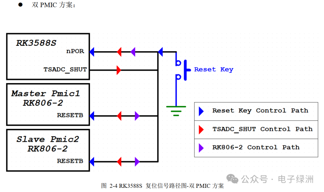
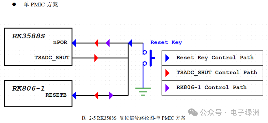
The RESETB pin of RK806-1/2 will, after all power supplies are powered up during the first power-on, delay the set time before transitioning from low to high level (open-drain output), completing the power-on reset process.
When RK806-1/2 is in working or sleep mode, if the RESETB pin is pulled low, RK806-1/2 will also restart, with the restart power-up sequence being the same as the first power-on.
——END——
In the jungle society, tears are never believed; no amount of complaints will help, and no one will pity you.
Recommended Reading
[Simulation Series] This circuit simulation software allows you to clearly see the direction and magnitude of current flow, with installation package download
[Rockchip Series] Rockchip RK3588S Hardware Design Guide – Minimum System Design for Clock Circuit
[Sensor Series] Security Camera Monitoring CMOS Image Sensor – Smart Way SMARTSENS-SC5336P
[Teardown Series] Yingshi CB2-4G 4G Unlimited Flow 3 Million Ultra-Clear Large Capacity Lithium Battery Indoor Smart Monitoring Home Camera AOV All-Day Recording
[Teardown Series] Yingshi’s Jingxiaodou Dual Camera 10 Million Camera Monitoring D220
Due to changes in the public account’s push rules, to prevent losing track of me, please like and star me. (Method: Go to the public account homepage, click the upper right corner “…”, then click to add to stars, thank you for your support!)
Like Share View AgainThank you for your “three consecutive” supportLimited time free scan code to join the group, exchange more technical and industry information