PCB Network News The impact of PCB warpage is well understood in the industry. It can prevent the installation of SMT electronic components, lead to poor contact between electronic components (including integrated circuits) and the solder joints on the printed circuit board, or cause some leads to be cut off or cut into the substrate during component installation; during wave soldering, some pads on the substrate may not contact the solder surface and thus cannot be soldered.
The causes of printed circuit board warpage include potential warping of the substrate (copper-clad laminate), but during the processing of printed circuit boards, thermal stress, chemical factors, and improper production processes can also lead to warpage.
Therefore, for printed circuit board manufacturers, the first step is to prevent warpage during the processing of printed circuit boards; secondly, there should be appropriate and effective methods for dealing with already warped PCBs.
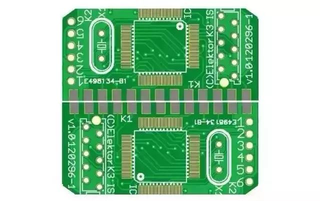
1. Preventing Warpage During PCB Processing
1. Prevent warpage caused by improper storage methods
(1) During storage, copper-clad laminates can absorb moisture, which increases warpage. The moisture absorption area of single-sided copper-clad laminates is large, and if the storage environment is humid, warpage will significantly increase. For double-sided copper-clad laminates, moisture can only penetrate from the product’s end face, with a smaller moisture absorption area and slower warpage changes. Therefore, for copper-clad laminates without moisture-proof packaging, attention should be paid to the storage conditions, reducing humidity, and avoiding placing the laminates bare to prevent increased warpage during storage.
(2) Improper placement of copper-clad laminates can increase warpage. For example, vertical placement or placing heavy objects on the laminates can exacerbate warpage deformation.
2. Avoid warpage caused by improper PCB circuit design or processing technology
If the PCB circuit pattern is unbalanced or if there is a significant asymmetry between the two sides of the PCB, where one side has a large area of copper, it creates significant stress, causing warpage. High processing temperatures or large thermal shocks during PCB fabrication can also lead to warpage. The impact of improper storage of copper-clad laminates is relatively easy for PCB manufacturers to solve by improving storage conditions and avoiding vertical placement and heavy pressure. For PCBs with large areas of copper in their circuit patterns, it is best to grid the copper foil to reduce stress.
3. Eliminate substrate stress to reduce PCB warpage during processing
During PCB processing, the substrate is subjected to heat multiple times and exposed to various chemicals. For example, after etching the substrate, it needs to be washed and dried, which involves heating; during pattern electroplating, heat is generated; after applying green oil and printing characters, it needs to be dried with heat or UV light; during hot air soldering, the substrate also experiences significant thermal shock. All these processes can cause PCB warpage.
4. During wave soldering or immersion soldering, high solder temperatures and prolonged operation times can also exacerbate substrate warpage. Improvements to the wave soldering process require cooperation from electronic assembly factories.
Since stress is the main cause of substrate warpage, many PCB manufacturers believe that pre-baking the copper-clad laminates (also known as H-Boarding) before use can help reduce PCB warpage. The purpose of H-Boarding is to allow the substrate’s stress to relax sufficiently, thereby reducing warpage during the PCB fabrication process.
The H-Boarding method is as follows: PCB manufacturers with the conditions use large baking ovens for H-Boarding. Before production, a large stack of copper-clad laminates is placed in the oven and baked for several hours to over a dozen hours at a temperature near the substrate’s glass transition temperature. PCBs produced from pre-baked copper-clad laminates exhibit significantly less warpage, resulting in a much higher product qualification rate. For smaller PCB manufacturers without such large ovens, the substrates can be cut smaller and then baked, but during the baking process, weights should be placed on the laminates to keep them flat during stress relaxation. The baking temperature should not be too high, as excessive temperatures can discolor the substrate, nor too low, as low temperatures require much longer to relax the substrate’s stress.
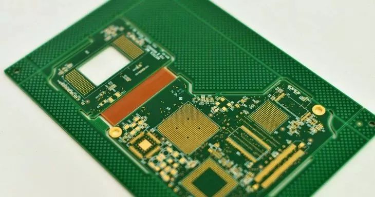
2. Methods for Flattening Warped PCBs
1. Timely flattening of warped boards during PCB processing
During PCB processing, boards with significant warpage should be selected and flattened using a roller flattening machine before proceeding to the next process. Many PCB manufacturers believe this practice effectively reduces the proportion of warped finished PCBs.
2. Flattening method for warped finished PCBs
For completed PCBs with significant warpage that cannot be flattened using a roller flattening machine, some PCB manufacturers place them in a small press (or similar fixture) and apply cold pressure for several hours to over a dozen hours to flatten the warped PCBs. However, from practical observations, this method is not very effective. One issue is that the flattening effect is minimal, and the flattened boards can easily rebound (i.e., return to their warped state).
Some PCB manufacturers heat the small press to a certain temperature before applying hot pressure to flatten the warped PCBs, which yields better results than cold pressure. However, if the pressure is too high, it can deform the wires; if the temperature is too high, it can cause defects such as discoloration of the solder mask or the substrate. Moreover, whether cold or hot pressure, it takes a long time (several hours to over a dozen hours) to see results, and the rebound ratio of warped PCBs after flattening is also high. Is there a better flattening method?
3. Bow-shaped mold hot pressure flattening method for warped PCBs
Based on the mechanical properties of polymer materials and years of practical experience, this article recommends the bow-shaped mold hot pressure flattening method. This involves creating several simple bow-shaped molds based on the area of the PCB to be flattened, and here we propose two flattening operation methods.
(1) Place the warped PCB in the bow-shaped mold and bake in the oven for flattening:
Place the warped side of the PCB against the curved surface of the mold, adjust the fixture screws to deform the PCB slightly in the opposite direction of its warpage, and then place the mold containing the PCB in a preheated oven for a period of time. Under heating conditions, the substrate’s stress gradually relaxes, enabling the deformed PCB to return to a flat state. However, the baking temperature should not be too high to avoid discoloration of the solder mask or yellowing of the substrate, nor too low, as low temperatures require a long time for the stress to fully relax.
Typically, the glass transition temperature of the substrate can be used as a reference baking temperature, as it is the point of phase transition for the resin. At this temperature, the segments of the polymer chains can rearrange, allowing the substrate’s stress to relax fully. Therefore, the flattening effect is significant. The advantage of using bow-shaped molds for flattening is that the investment is minimal, as all PCB manufacturers have ovens, and the flattening operation is straightforward. If there are many warped boards, making several sets of bow-shaped molds allows for multiple molds to be placed in the oven at once, and the baking time is relatively short (about tens of minutes), thus improving the efficiency of the flattening work.
(2) First soften the PCB in the oven and then clamp it in the bow-shaped mold for flattening:
For PCBs with minor warpage, they can be placed in a preheated oven (the temperature setting can refer to the substrate’s glass transition temperature and the time required for the substrate to soften in the oven). Generally, the baking temperature for fiberglass substrates should be higher, while for paper substrates, it can be lower; thicker boards can be baked at slightly higher temperatures, while thinner boards can be baked at slightly lower temperatures; for PCBs that have been coated with solder mask, the baking temperature should not be too high. After baking for a certain period, several to a dozen boards can be removed and clamped in the bow-shaped mold, adjusting the pressure screws to deform the PCB slightly in the opposite direction of its warpage. After the board cools and takes shape, the mold can be removed to obtain the flattened PCB.
Some users may not be familiar with the glass transition temperature of the substrate. Here, we recommend baking reference temperatures: for paper substrates, the baking temperature is 110°C to 130°C, and for FR-4, it is 130°C to 150°C. During flattening, conduct several small tests on the selected baking temperature and time to determine the optimal baking conditions for flattening. Longer baking times ensure that the substrate is thoroughly baked, leading to better flattening effects, and the rebound rate of the PCB after flattening is lower.
PCBs that have undergone bow-shaped mold flattening exhibit low rebound rates; even after wave soldering, they can maintain a relatively flat state; and the impact on the PCB’s appearance and color is minimal.
PCB warpage is a significant headache for PCB manufacturers, as it not only reduces yield rates but also affects delivery times. By adopting the bow-shaped mold hot flattening method with reasonable and suitable processes, warped PCBs can be flattened, alleviating delivery time concerns.
Source: Ruibo Doctor R&D Engineering
Recommended Hot Articles
Gathering Industry Elites to Explore Development Paths—Successful GPCA/SPCA Council Meeting
[Company Visit] Shenghong Technology: Smart Factory Creates New Growth Momentum, Building a Zero-Emission PCB Benchmark Enterprise
[Company Honor] Excellent! Jingwang Electronics Has Been Awarded Honeywell’s Global “Excellent Supplier” for Five Consecutive Years
[Private Economy] Three Issues That Cannot Be Ignored Regarding Private Enterprises
[Macro Perspective] Vietnam’s Advantages in the Rapid Growth of PCB Output Value in 2017
[Company News] Xingsen Technology Plans 237 Million Yuan to Expand Existing Packaging Substrate Production Lines
[Company Announcement] Helitai Officially Changes Ownership! 30% of Fujian State-owned Assets Transferred
[Charity] Chongda Scholarships: Helping Impoverished Students Succeed
[Company Research Report] Yidun Electronics: Riding the Wave of AI Driving New Energy Vehicles and 5G Construction in Medical Control
[Hot Topic] China Suspends Additional Tariffs on U.S. Automobiles for Three Months! Involving 211 Tax Items