The Artix 7 series FPGA provides many DSP hardware units that can be configured for floating-point operations.In the Vivado IP configuration interface, the clock cycle for the module can be selected, and data can be read out after a specified number of clock cycles. The Floating Point IP resource user manual from Vivado.However, it is somewhat strange that Xilinx’s manual only mentions that this feature can be used for hardware reuse by increasing cycles to reduce hardware resources, but does not mention the impact on timing.
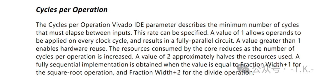 The manual only describes hardware reuse.I checked other data manuals and forums, and it seems there is also no discussion on timing and performance, so I am curious about the impact of this clock cycle option on hardware timing, and I will conduct a simple experiment to verify it.The configuration is very simple; I directly initialize an FP32 DSP unit under the toplevel and configure it in a three-input multiply-accumulate mode.To prevent inaccurate optimizations, the AXIS inputs and outputs of the module are directly connected to the board’s IO pins.The AXIS clock of the IP module is provided by a PLL, and we verify that this design can close timing under different clock cycle settings.I originally planned to run it simply using the Vivado GUI, but found that running two parameters took a long time, so I wrote a simple Python program to drive the Vivado TCL script to automatically create project files with different configurations.The code is available here:
 https://github.com/ucb-bar/Vivado-Floating-Point-IP-Performance-TestAfter running overnight and getting a good night’s sleep, I obtained the following results.Here is the graph I got:
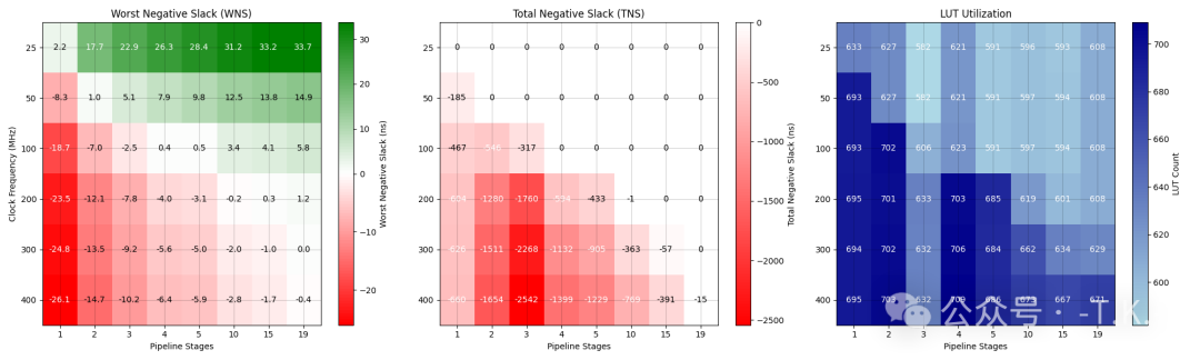 The overall trend meets expectations; as the pipeline depth increases, the frequency that this IP block can achieve is also higher.Surprisingly, the LUT usage is very low at a pipeline depth of 3, and I am not sure why.Additionally, it is unclear why the LUT usage increases with frequency; it may be related to the distribution of the clock tree….?