This article introduces some practical basic techniques for PCB-level hardware reverse engineering, which can be used by researchers and white hat groups to analyze unknown hardware. The hardware security laboratory operated by SEC Consult is part of the SEC Consult security lab. The research presented below is just the tip of the iceberg among many studies conducted by the hardware lab.
Today, we live in a world dominated by embedded devices. Everyone may be living under various forms of surveillance and monitoring. Routers, network cameras, smartphones, and other embedded devices affected by security vulnerabilities are highly susceptible to attacks. The recent outbreak of the Mirai virus and other IoT malware further illustrates this point. Whether out of curiosity or at the request of customers to enhance product security, a deep audit of the firmware of such devices requires disassembly to find debugging interfaces. Only through debugging and running the system can we reveal its hidden aspects. Due to the potentially destructive nature of this process, it often results in damage to the device. Therefore, to conduct in-depth analysis, it is not enough to prepare just one device!
How to start with a familiar device?
To save on expensive embedded analysis costs, a simple and quick method is to replace the firmware. Large companies can easily commission security consulting firms to test the built-in firmware of products before introducing large batches of IoT devices, thereby minimizing security risks. However, for users and hobbyists, the options are limited, and the firmware they can install often comes from third parties like OpenWRT. Although the performance of these firmware may not necessarily surpass that of the native firmware (which is developed for the proprietary chip instruction set), they are indeed superior in terms of security. When we complete the task of auditing the security of known devices, the hardware analysis part is usually simplified to searching for relevant information on online forums (often the OpenWRT Wiki).
Hardware Hacking – Identifying Debugging Interfaces of Undocumented Devices
Flashing firmware onto a completely unknown ordinary device is an almost impossible task. Therefore, we need to gradually dissect the hardware circuit to check the firmware used and detect security vulnerabilities in the firmware. However, reverse engineering hardware circuits is not a simple task, especially for proprietary chip circuits, but some basic analysis techniques are still applicable. In our example, the Broadcom SoC serves as the core component of the Belkin F9 K1106as (Belkin) wireless repeater. We are using this device as an example not because of any particular interest in it, but because its chip set is also used in many other community-supported devices. To identify the pins of this SoC, we connect it to a dedicated power supply. Opening the device’s casing reveals the PCB. Our first goal is to establish a serial connection to the device to obtain a shell or at least access the bootloader.
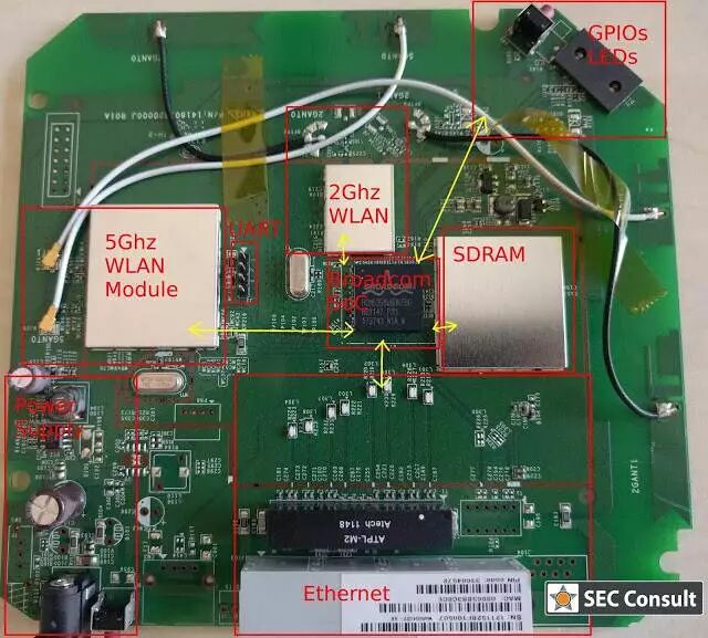
Figure: PCB diagram of Belkin F9 K1106as and its various modules
The simplest way to identify modules protected by metal shields is to remove the shield.
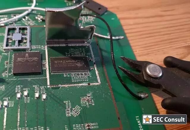
Figure: Using pliers to open the electrostatic shield
To reverse engineer the debugging pin interfaces hidden on the PCB, we do not need to remove the entire shield. By utilizing the UART interface exposed on the PCB (Note: Universal Asynchronous Receiver-Transmitter, see Baike), we can achieve initial debugging, as connecting the UART directly to an FT2322H board set to 11520 Baud 8n1 as a terminal can provide access to the root shell. Compared to other interfaces, UART is relatively easy to identify, as it only has two pins, the receive and transmit pins. Serial communication is not always UART, but this can help us narrow down the possibilities. A set of 3-5 pins is usually reserved for UART interfaces during PCB development.
The typical pin arrangement for UART is (GND|RX|TX|VCC) or (GND|TX|RX|VCC).
So where is JTAG (Note: Joint Test Action Group, see Baike)? This standard allows developers or experienced hackers to easily control the CPU, debug the SoC during runtime, read and program flash, and run self-test diagnostics. This question can be answered with a JTAG brute force tool. The tools developed by SEC Consult (including hardware and software) come with this functionality, and of course, there are many tools available online for this purpose. Since effective debugging pins typically consist of 4-5 pins, the 10 pins on the top of the PCB look like JTAG.
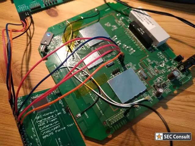
Figure: Brute force detection of JTAG pins
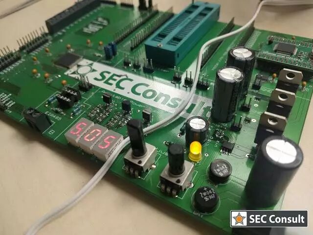
Figure: Hardware analysis tool “SEC Xtractor” developed by SEC Consult security lab
After brute force detection, we finally identified the pins! To maintain integrity, we also marked the UART interface.
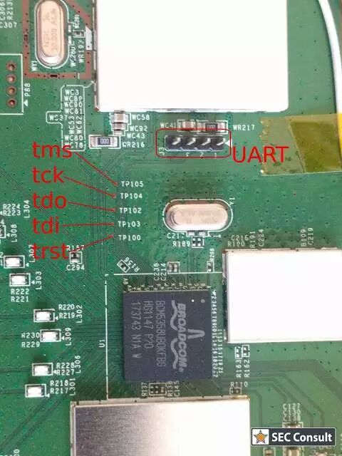
Figure: JTAG pins
As for the JTAG adapter, a cheap mini FT2322H module is used.
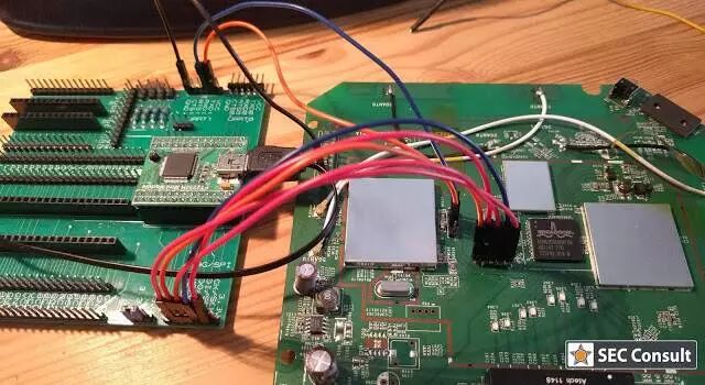
Figure: Connecting to JTAG via mini FT2232H module
The request to connect to OpenOCD yielded the following result:
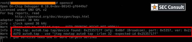
Figure: OpenOCD output
The chip appears to have a 32-bit instruction register with an ID of 0x2535717f. Previously, we only knew that the Broadcom SoC was labeled BCM5358UB0KFBG. Now, we have more understanding—albeit specific to this device; the JTAG interface can be used to control the chip and access the system at a low level.
Hardware Hacking – Extracting Firmware
Extracting firmware is the final step in completing the information pool for this SoC. A Macronix serial flash chip is installed on the back of the PCB. It only takes a few minutes with flashrom and FT2322H to read its contents. The pin definitions can be quickly found from the datasheet:
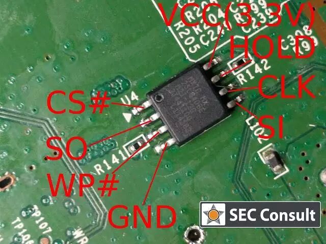
Figure: Macronix SPI flash chip pinout
After removing the flash chip from the PCB, place it on an adapter and start flashrom:
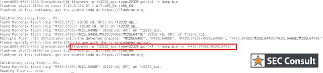
Figure: Reading SPI memory with flashrom
The dump file includes the entire program memory and temporary data (NVRAM). Rewriting the firmware with flashrom and soldering the chip back is another method for flashing third-party firmware. By calling “binwalk-Adump.bin”, we obtain many “MIPSEL” (MIPS little endian) instructions, which leads us to hypothesize that the Broadcom SoC is based on a generic MIPSEL32 CPU. SOP packaged serial flash chips are the easiest to read, while more challenging NAND and NOR flash chips are difficult to operate due to their complex interfaces, small packages, and numerous pins.
Preliminary analysis of the dump file using IoT Inspector shows that the firmware has some basic security risks, while also obtaining information about the software used by the device. Since we are analyzing an older device, some security vulnerabilities can be traced back to 2007:
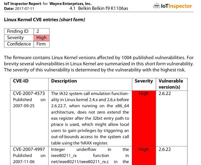
Figure: Excerpt from IoT Inspector report
Hardware Hacking – Reverse Engineering SoC Pins
As previously mentioned, if we obtain the pin definitions of the SoC, we can reverse engineer any device using BCM5358UB0KFBG. For this purpose, in most cases, we can use a hot air gun to desolder the BGA packaged chip.
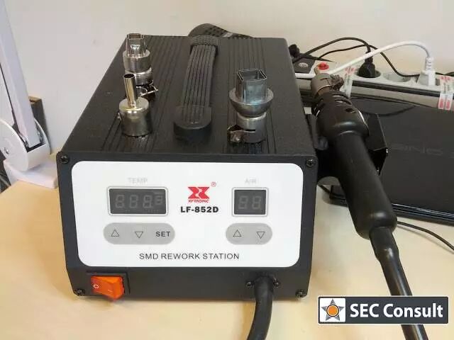
Figure: Hot air gun rework station
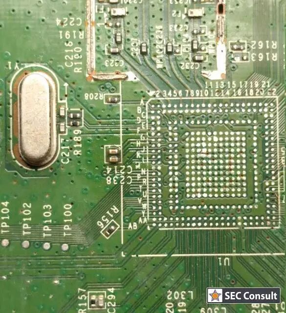
Figure: Belkin PCB after removing the SoC
Based on the pin connections of the SoC, combined with relevant information from the datasheet and measurements of pin voltages to ground/power (GND/VCC) and logical deductions, we derive the functional definitions of some important pins of the chip.
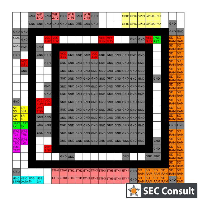
Figure: Functional definitions of some pins of the BCM5358U0KFBG chip
Clearly, the BCM535x series chips have similar pin definitions.https://wikidevi.com collects information on computer hardware, including the Broadcom SoC series. We found the following entry:

Figure: Source: https://wikidevi.com
Observing images of other routers containing such chips reveals that the pin functions are quite similar.
The Wikidevi website contains a wealth of information on hardware, and the documentation provided by manufacturers is also very detailed. China seems to be the only country producing routers for various brands.
Hardware Hacking – Supply Chain from China
All these electronic products made in China, including chips, peripherals, routers, etc., are often assembled by the same factory. The result is evident; the quality of these products is at a similar level, and some factories also produce products for competing market suppliers. Let’s take a look at the internal images of the Asus RT-N53 router and the Belkin F9 K1106 wireless repeater. The markings on the PCB are almost identical, aren’t they?
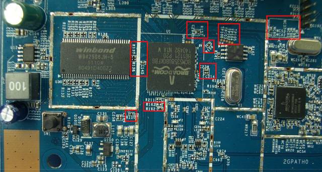
Figure: Asus PCB, Source: https://apps.fcc.gov/
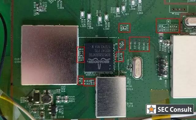
Figure: Belkin PCB
Coincidence? Not really. The fonts of these markings are the default settings of ELCAD (Electronic Computer Aided Design) software, and developers would not change them unless required. This means that the same template is reused for the development of Asus PCBs and even more products from other suppliers. Therefore, the same ODM (Original Design Manufacturer) is responsible for the design and manufacture of products for various brands, including Belkin.
This production form is not uncommon in embedded device manufacturing, especially for companies from the US. Most of the firmware is also developed by Asian suppliers based on standard or customized SDKs.
The increasing number of backdoor incidents are mostly logical flaws—as we have seen before:
-
http://blog.sec-consult.com/2017/06/ghosts-from-past-authentication-bypass.html
-
http://blog.sec-consult.com/2016/12/backdoor-in-sony-ipela-engine-ip-cameras.html
-
http://blog.trendmicro.com/trendlabs-security-intelligence/netis-routers-leave-wide-open-backdoor/
-
http://www.devttys0.com/2013/10/from-china-with-love/

This article was translated by the Kanxue Translation Team StrokMitream, sourced from SecConsult@Thomas Weber. Please indicate the source from the Kanxue community when reprinting.

Popular Reads
-
Using x64dbg+VS2015 Spy++ to Remove Ad Pop-ups
-
Analyzing SO Loading from Android Source Code
-
A Report on the Analysis of a lpk.dll Virus
-
A Brief Discussion on Virtual Machine Protection Technologies
Click to read the original text/read, and more valuable content awaits you~