Safety Distance Requirements
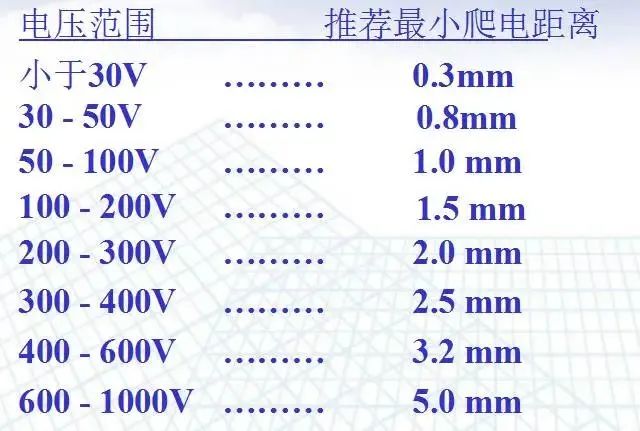
This includes electrical clearance (air gap), creepage distance (surface distance), and insulation penetration distance.
1. Electrical clearance: The shortest distance measured along the air between two adjacent conductors or between a conductor and the surface of an adjacent motor casing.
2. Creepage distance: The shortest distance measured along the insulating surface between two adjacent conductors or between a conductor and the surface of an adjacent motor casing.
1. Requirements for creepage distance and electrical clearance:
1. Creepage distance: For input voltages of 50V-250V, the distance before the fuse L—N ≥ 2.5mm; for input voltages of 250V-500V, L—N ≥ 5.0mm; electrical clearance: for input voltages of 50V-250V, L—N ≥ 1.7mm; for input voltages of 250V-500V, L—N ≥ 3.0mm; no requirements after the fuse, but maintain a certain distance to avoid short circuit damage to the power supply;
2. The distance from the AC side to the DC part ≥ 2.0mm;
3. The distance from the DC ground to ground ≥ 4.0mm, such as the distance from the primary side ground to the earth;
4. The distance from the primary side to the secondary side ≥ 6.4mm; for components like optocouplers and Y capacitors with pin spacing ≤ 6.4mm, grooves should be opened;
5. The distance between transformer stages should be ≥ 6.4mm, and ≥ 8mm for reinforced insulation.
 EMC and Interference Resistance1. Long Line Interference Resistance
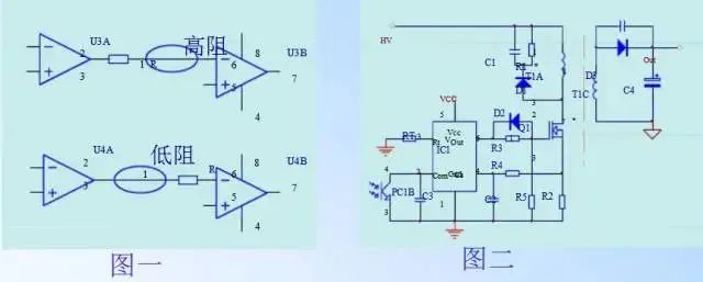 In Figure 2, during PCB layout, the driver resistor R3 should be close to Q1 (MOSFET), and the current sensing resistor R4 and C2 should be close to pin 4 of IC1, as mentioned in Figure 1, R should be as close as possible to the operational amplifier to shorten the high-impedance line. The input impedance of the operational amplifier is very high and is easily affected by interference. The output impedance is relatively low and is less susceptible to interference. A long line acts like a receiving antenna, easily introducing external interference.
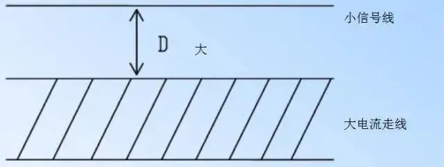
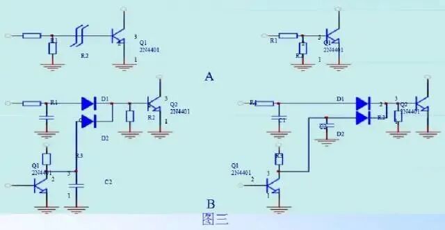 In layout A of Figure 3, R1 and R2 should be placed close to transistor Q1, as Q1 has a very high input impedance, and a long base line is susceptible to interference, so R1 and R2 should not be far from Q1.In layout B of Figure 3, C2 should be close to D2 because the input impedance of transistor Q2 is very high. If the line from Q2 to D2 is too long, it is susceptible to interference, so C2 should be moved near D2.2. Small signal lines should be kept as far away from high current lines as possible, avoiding parallel routing, D >= 2.0mm.
 3. Small signal line handling: PCB routing should be concentrated to reduce board area and improve interference resistance.4. The area enclosed by a current loop should be minimized.
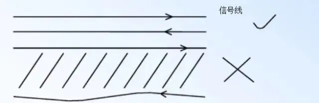 5. Optocoupler devices are susceptible to interference and should be kept away from strong electric fields and magnetic field devices, such as high current lines, transformers, and high potential pulsing devices.6. For multiple ICs powered, pay attention to Vcc and ground lines.
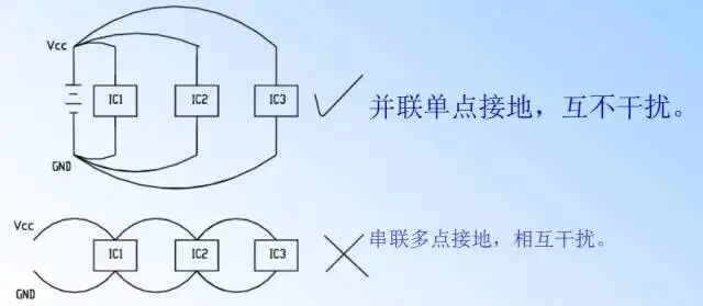 7. Noise Requirements1. Minimize the area surrounded by high-frequency pulse currents, as shown below (Figures 1 and 2).
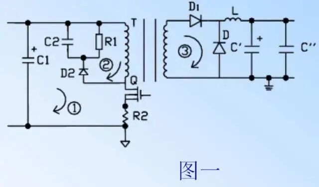 Typical board layout:
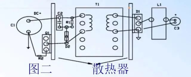 2. Filter capacitors should be placed as close as possible to the switching transistors or rectifier diodes, as shown in Figure 2, C1 should be close to Q1, C3 close to D1, etc.3. The area where pulse currents flow should be kept away from input and output terminals to separate noise sources from input and output ports.
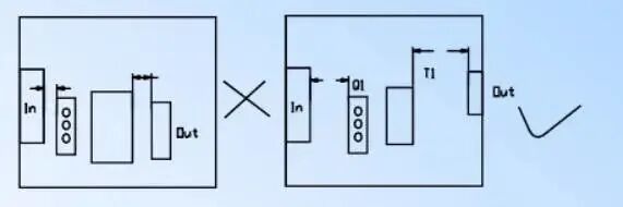
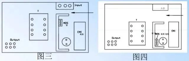 Figure 3: The MOSFET and transformer are too close to the input, causing electromagnetic radiation energy to directly affect the input terminal, resulting in EMI test failure.Figure 4: The MOSFET and transformer are far from the input, increasing the distance of electrical and magnetic radiation energy from the input terminal, thus allowing EMI conduction to pass.4. Control circuits should be separated from power circuits, using a single-point grounding method, as shown in Figure 5.
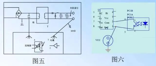 Grounding of components around the control IC should connect to the IC’s ground pin; then lead out to the large capacitor ground line. The ground of the optocoupler’s pin 3 should connect to pin 1 of the IC, and pin 4 should connect to pin 2 of the IC, as shown in Figure 6.5. If necessary, the output filter inductor can be placed on the ground loop.6. Use multiple capacitors with low ESR in parallel for filtering.7. Use copper foil for low inductance and low resistance wiring; there should not be excessively long parallel lines between adjacent lines, and routing should avoid parallel and crossing, using vertical routing instead. The line width should not change abruptly, and routing should not have sudden corners (i.e., ≤ right angles). (Parallel routing of the same current loop can enhance interference resistance.)8. Interference Resistance Requirements:1. Minimize the length of connections between high-frequency components, and try to reduce their distributed parameters and mutual electromagnetic interference. Susceptible components should not be too close to strong interference devices, and input/output components should be kept as far away as possible.2. If there is a significant potential difference between certain components or wires, increase the distance between them to avoid discharge leading to unexpected short circuits.Overall Layout and Routing Principles1. Overall Layout1. Heat sinks should be evenly distributed, and airflow should be good.
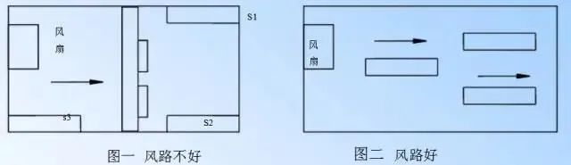 2. Capacitors, ICs, and other components should maintain a distance from heat-generating components (heat sinks, rectifier bridges, continuation inductors, power resistors) to avoid being affected by heat.3. Current loops: To facilitate wiring, the distance between lead holes should not be too far or too close.4. Input/output, AC/socket should ensure that the lengths of the two wires are consistent, leaving some space margin, paying attention to the position occupied by the plug wire clip, and ensuring ease of plugging and unplugging. Output wire holes should be neat for easy soldering.5. Components should not touch each other; the screw positions of MOSFETs and rectifiers should not collide with other components to simplify assembly processes. Capacitors and resistors should not touch the pressure strips or screws; when laying out the board, consider the positions of screws and pressure strips in advance, as shown in Figure 3:
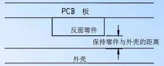
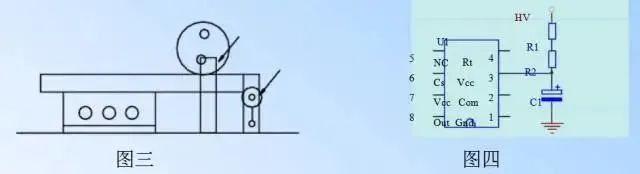 6. Except for temperature switches, thermistors, etc., key components sensitive to temperature (such as ICs) should be kept away from heat-generating components. Components that generate significant heat should maintain a certain distance from components that affect the overall lifespan, such as capacitors.7. For adjustable components like potentiometers, adjustable inductors, variable capacitors, and micro switches, the layout should consider the structural requirements of the entire machine. If adjustments are made inside the machine, they should be placed conveniently on the PCB; if adjustments are made outside, their position should correspond to the position of the adjustment knob on the chassis panel.8. Leave space for the positioning holes of the printed PCB board supports.9. Components located at the edge of the circuit board should generally be at least 2mm away from the edge of the circuit board.10. Output wires, indicator wires, and fan wires should be aligned, with consistent polarity corresponding to the panel.11. General layout: Do not connect high voltage on small boards; place high voltage components on larger boards. If there are special circumstances, safety regulations must be considered. For example, place R1 and R2 on the larger board and introduce a low voltage line.12. The primary heat sink should maintain a distance of more than 5mm from the shell (except for mica sheets).13. When laying out the board, pay attention to the height of components on the back side. As shown in Figure 5:
 14. The primary and secondary Y capacitors and transformer cores should pay attention to safety regulations.2. Layout Requirements for Unit Circuits1. Arrange the positions of various functional circuit units according to the flow of the circuit to facilitate signal flow and keep the signal direction as consistent as possible.2. Layout should be centered around the core components of each functional circuit, with components evenly and compactly arranged on the PCB to minimize and shorten the connecting leads between components.3. When working at high frequencies, consider the distributed parameters of components. Generally, circuits should arrange components in parallel as much as possible, which not only looks good but also makes soldering easier and is conducive to mass production.3. Routing Principles1. Wires used for input and output should avoid being adjacent and parallel; it is best to add ground lines between them to avoid feedback coupling.2. The width of the routing is mainly determined by the adhesion strength between the wire and the insulating substrate and the current flowing through them. When the copper foil thickness is 50μm and the width is 1mm, a current of 1A will not cause a temperature rise of more than 3°C. Based on this, a 2-ounce (70μm) thick copper foil with a width of 1mm can carry a current of 1.5A without exceeding a temperature rise of 3°C (Note: natural cooling).3. The electrical clearance width between the input control circuit part and the output current and control part (i.e., the distance between small current routing and output routing) should be: 0.75mm–1.0mm (Min 0.3mm). The reason is that if the copper foil and pads are too close, it can easily cause short circuits and adverse electrical interference reactions.4. ROUTE line corners should generally be rounded; right angles and sharp angles can affect electrical performance in high-frequency circuits.5. Power lines should be thickened according to the size of the line current to reduce loop impedance, while ensuring that the routing of power lines and ground lines is consistent with the direction of data transmission, minimizing the enclosed area, which helps enhance noise resistance.A: The grounding of heat sinks is mostly done using single-point grounding to improve noise suppression capability, as shown in the figure below:
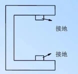 Before change: Multi-point grounding forms a magnetic field loop, failing EMI tests.
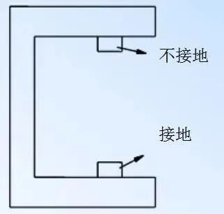 After change: Single-point grounding has no magnetic field loop, passing EMI tests.6. Routing of filter capacitors A: Noise and ripple are completely filtered out by the filter capacitor.
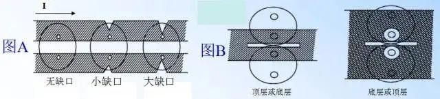
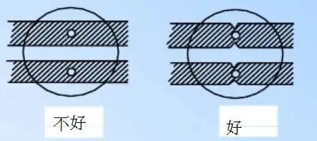 B: When the ripple current is too large, multiple capacitors are connected in parallel. The ripple current passing through the first capacitor generates more heat than the second and third, making it easy to damage. When routing, try to evenly distribute the ripple current to each capacitor, as shown in routing A and B. If space permits, routing can also be done as shown in Figure B.
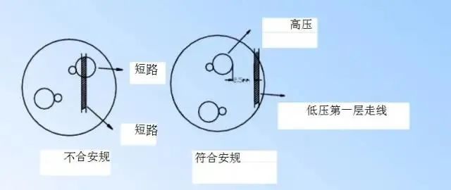
 7. High voltage high frequency electrolytic capacitor leads have a rivet, as shown in the figure below, which should maintain a distance from the top layer routing copper foil and comply with safety regulations.
 8. Weak signal routing should not run under inductors, current loops, and other devices.
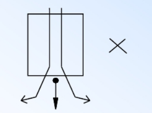 Current sampling lines can cause faults during mass production if they come into contact with the magnetic core and line copper foil.10. High voltage lines should not run under metal film resistors; low voltage lines should be routed in the middle of the resistors to avoid short circuits if the resistors are damaged.11. Soldering:A: Add solder to narrow areas of power line copper foil;B: The RC absorption loop requires soldering due to high current and for heat dissipation;C: Add solder under heat-generating components for heat dissipation, but do not press down on the solder pads.12. Signal lines should not pass through transformers, heat sinks, or MOSFET pins.13. If the output is superimposed, the differential mode inductor’s front capacitor should connect to the front ground, and the differential mode inductor’s rear capacitor should connect to the output ground.
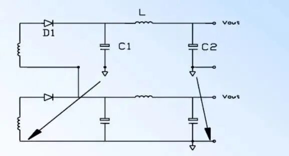 14. Areas where high-frequency pulse currents flow:
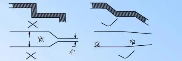
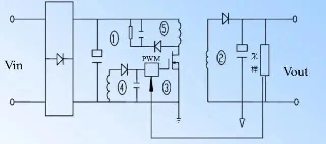 A: Minimize the area surrounded by high-frequency pulse currents, as indicated by the five loops marked in the figure above.B: Power lines and ground lines should be kept close together to reduce the area they enclose, thereby minimizing electromagnetic interference caused by external magnetic field loops and reducing the electromagnetic radiation of the loop to the outside.C: Large capacitors should be kept as close to the MOSFET as possible, and the output RC absorption loop should be kept as close to the rectifier as possible.D: The routing of power lines and ground lines should be thickened and shortened to reduce loop resistance, with smooth corners and no abrupt changes in line width, as shown in the figure below:
 E: The area where pulse currents flow should be kept away from input and output terminals to separate noise sources from outputs.
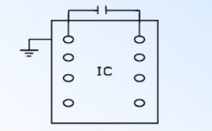
 F: The oscillation filter decoupling capacitor should be close to the IC ground, and the ground line should be short.
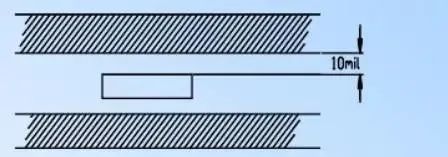
 15. The vertical transformer magnetic core of manganese copper wire and the power resistor heat sink should not have the first layer of lines running underneath.16. There should be a distance of more than 10MIL between grooves and copper foil routing, paying attention to safety regulations for the metal parts on the upper and lower layers.
 17. The same name terminals of driving transformers, inductors, and current loops should be consistent.18. For double-sided boards, add more vias at high current routing points, and vias should be soldered to increase current-carrying capacity.19. On single-sided boards, jumpers should not touch other components. If jumpers connect to high voltage components, they should maintain a certain safety distance from low voltage components. They should also maintain a distance of more than 1mm from heat sinks.4. Case AnalysisSwitching power supplies are becoming smaller, their operating frequencies are increasing, and the density of internal components is also increasing, which raises the requirements for interference resistance in PCB routing. The following are the problems found and solutions based on some case routings:1. Overall layout Case 1 is a six-layer board. The initial layout placed the control part on the component side and the power part on the solder side. During debugging, significant interference was found, caused by the unreasonable placement of the PWM IC and optocoupler, as shown:
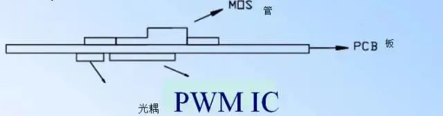 As shown in the figure above, the PWM IC and optocoupler are placed under the MOSFET, with only a 2.0mm PCB separating them, allowing the MOSFET to directly interfere with the PWM IC. The improvement was made by:
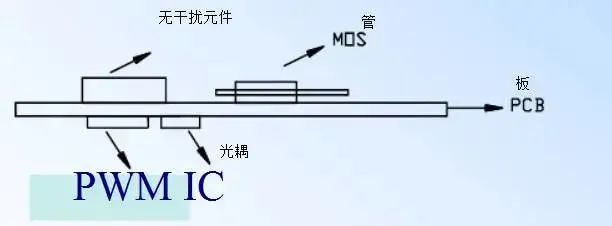 Moving the PWM IC and optocoupler away, ensuring that there are no devices with pulsing components above them.2. Routing Issues: Power routing should be minimized to reduce the area enclosed by the loop and avoid interference. The area enclosed by small signal lines should be small, such as the current loop:
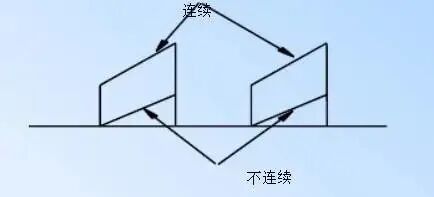
 The larger the area enclosed by lines A and B, the more interference they receive. This is because it is feedback current; lines A and B should have a short feedback coupling and should not cross or run parallel to pulsing signals.
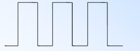
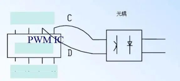 The current sampling line of the PWM IC chip should be routed as far away as possible from the drive line and synchronization signal line, and should not run parallel to them, otherwise they will interfere with each other. The current waveform is:
 The PWM IC drive waveform and synchronization signal voltage waveform are:
 Thermal Design SectionNote: The small board should not be too close to the transformer.
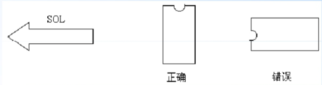
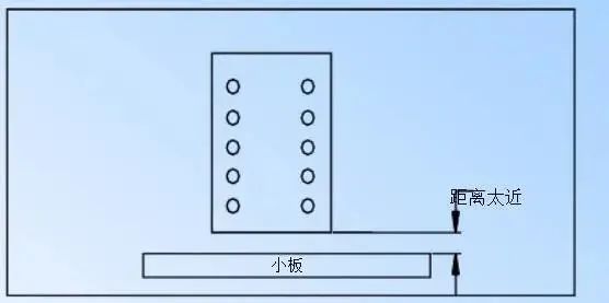 The small board being too close to the transformer can cause semiconductor components on the small board to easily overheat and be affected.Process Handling SectionEach PCB must have arrows indicating the direction of passing through the soldering furnace:
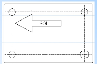 In layout, the direction of DIP packaged ICs must be perpendicular to the direction of passing through the soldering furnace, not parallel, as shown in the figure below. If layout difficulties arise, horizontal placement of ICs (SOP packaged ICs should be placed in the opposite direction to DIP) is allowed.
 The routing direction should be horizontal or vertical, and transitions from vertical to horizontal should be at a 45-degree angle. If the width of the copper foil entering a round pad is smaller than the diameter of the round pad, a teardrop should be added. Routing should be as short as possible, especially for clock lines, low-level signal lines, and all high-frequency loop routings. The ground and power supply systems of analog and digital circuits should be completely separated. If there are large areas of ground and power lines on the printed board (areas exceeding 500 square millimeters), local windows should be opened, as shown in the figure below:
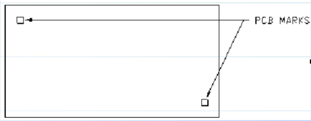
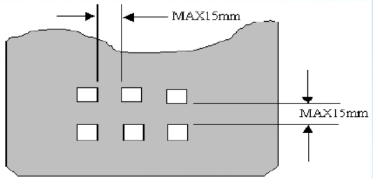 Horizontal inserted components (resistors, diodes, etc.) must have a center distance of 300mil, 400mil, and 500mil. (If not necessary, 240mil can also be used, but only for IN4148 type diodes or 1/16W resistors. 1/4W resistors start from 10.0mm.) The center distance between jumper pins must be 200mil, 300mil, 500mil, 600mil, 700mil, 800mil, 900mil, and 1000mil. The diameter of heat dissipation holes on the PCB should not exceed 140mil.If there are Φ12 or square holes larger than 12MM on the PCB, a cover to prevent solder from flowing out must be made, as shown in the figure (the hole gap is 1.0MM).On PCBs with surface mount components, correction marks (MARKS) must be set to improve the mounting accuracy of surface mount components, and each board must have at least two marks, located at a pair of diagonally opposite corners, as shown in the figure:
 Spacing for SMD components:
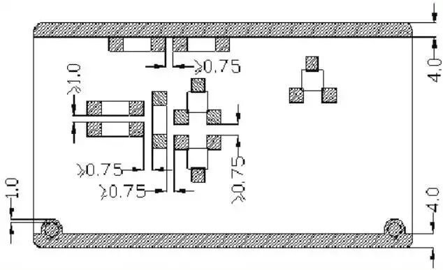 The distance between SMD components and the leads of electrical insertion components, as shown in the two figures below: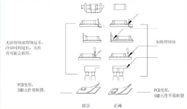
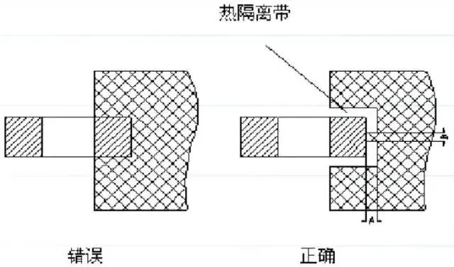
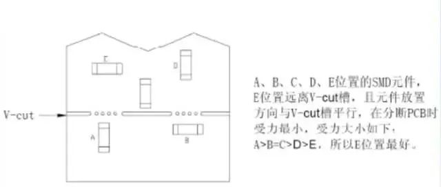 When connecting SMD device leads to large copper foils, thermal isolation treatment should be performed, as shown in the figure below:
 The center hole of the component pad should be slightly larger than the diameter of the device lead. If the pad is too large, it can lead to cold solder joints. The outer diameter D of the pad should generally be no less than (d+1.2) mm, where d is the lead hole diameter. For high-density digital circuits, the minimum pad diameter can be taken as (d+1.0) mm, and pads with a hole diameter greater than 2.5mm should be appropriately enlarged. Components should be neatly arranged, and their directions should be as consistent as possible. For SMD components on the PCB, the long axis centerline should be arranged perpendicular to the long axis centerline of the PCB to avoid breakage.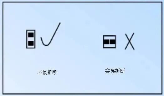
Copyright NoticeThis article is copyrighted by the original author and does not represent the views of this account. The articles pushed by this account are for sharing purposes only and do not represent the stance of this account. If there are copyright issues, please contact us for deletion.