Overview of Mainstream ADAS/AD Domain Control Chip Platforms
1. ADAS/AD System Solutions
(1) L0-L2 Level ADAS SolutionsAs mentioned earlier, most early L0-L2 level ADAS systems are based on a distributed controller architecture. The entire ADAS system consists of 4-5 ADAS subsystems, each of which is usually an all-in-one solution (which can be viewed as a smart sensor). Each subsystem exclusively occupies the sensors configured, and they are usually independent of each other.Taking the Intelligent Front Camera Module (FCM) as an example, the entire subsystem ECU motherboard contains two chips: one is the Safety Core; the other is the Performance Core. The Safety Core is generally an MCU like Infineon’s TC297/397, which carries control tasks and therefore requires a high level of functional safety; the Performance Core is usually a multi-core heterogeneous MPU with higher performance computing power, which will carry a large number of computing tasks.Below is a summary of the L0-L2 level solutions:
L0 Level Solution: Implements various ADAS warning functions, such as: FCW, LDW, BSW, LCA, etc. It is a distributed architecture, usually consisting of major hardware modules such as FCM, FCR, SRRs, AVS, APA, etc.
L1 Level Solution: Completes various ADAS single longitudinal and single lateral control functions, such as: ACC, AEB, LKA, etc. It is also a distributed architecture, and the hardware module composition is roughly the same as the L0 level solution.
L2 Level Solution: Completes ADAS longitudinal + lateral combined control functions. For example: based on the FCM + FCR fusion system, which fuses forward visual perception and front radar target perception information to achieve TJA/ICA functions; or based on the AVS + APA fusion system to achieve automatic parking functions.
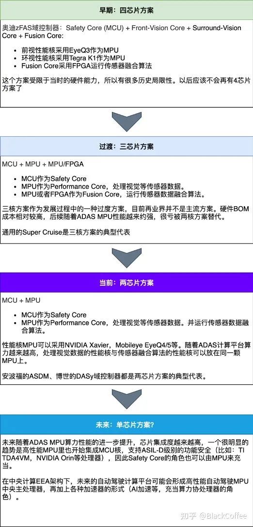
(2) L2+ Level ADAS SolutionsDistributed architecture ADAS systems have two fatal drawbacks:1) Each subsystem is independent and cannot perform deep fusion between multiple sensors.2) Each subsystem exclusively occupies the sensors configured, which makes it impossible to achieve complex functions across multiple different subsystem sensors.As the vehicle EE architecture evolves to a domain-centralized EEA, the ADAS domain controller is equipped with a higher integration and higher performance computing processor platform, which can support more complex sensor data fusion algorithms to achieve higher-level ADAS functions, such as: HWP, AVP, etc.The centralized ADAS domain controller solution has transitioned from the earliest four-chip solution, to a three-chip solution, and then to the current mainstream two-chip solution in the industry, as shown in the following Figure 3-5: Evolution History of ADAS Domain Controller SolutionsThe following figure illustrates a typical vehicle-mounted ADAS domain functional structure diagram. Regardless of how the hardware solutions change, the functional structure that each solution needs to achieve is similar. Typical Vehicle-mounted ADAS Domain Functional Structure Diagram
2. Mobileye EyeQ Series Chip Solutions
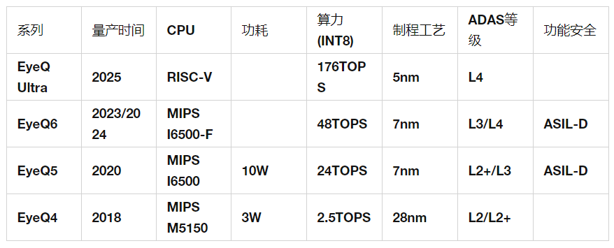
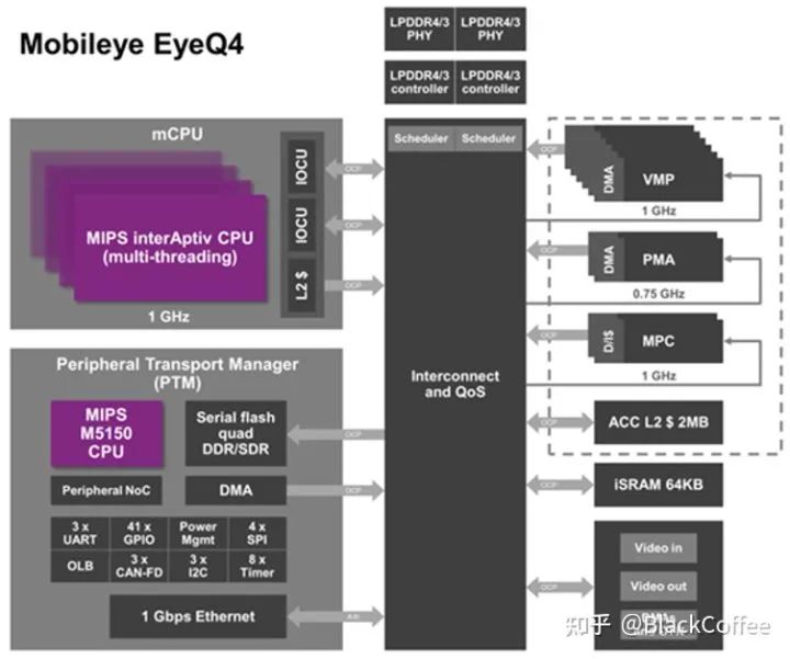
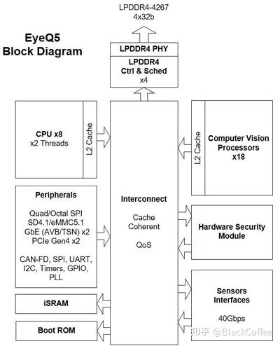
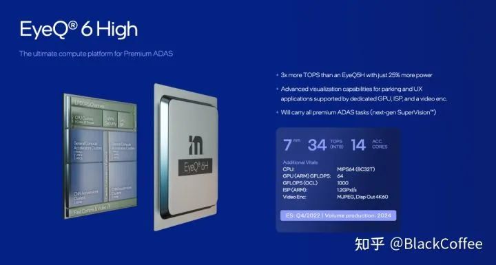
Established in 1999, Mobileye is a global leader in providing ADAS/AD solutions based on visual algorithm analysis and data processing from Israel. As of the end of 2021, its EyeQ series chip products have shipped nearly 100 million units in total. Despite being suppressed by Nvidia and Qualcomm in the L3/L4 field, it remains dominant in the mainstream L2 level ADAS market, with a market share as high as 75%. The shipment volume in 2021 reached 28.1 million units.Mobileye has always adopted a hardware-software integrated ADAS solution model that binds “sensors + chips + algorithms.” The advantage of this “black box” business model is a short development cycle, allowing customers to quickly launch products, which is favored by traditional OEMs or Tier 1 manufacturers that have transitioned later or have weaker software/algorithm capabilities. However, the downside is that it leads to a decrease in customer development flexibility, making it difficult to meet the demand for differentiated customized products. More and more OEMs hope to adopt a more open platform, separating “chips and algorithms, using programmable chips to achieve continuous algorithm iteration and upgrades through OTA.” This is also the idea behind software-defined vehicles.Below is the basic situation of its EyeQ4/5/6 three generations of products:(1) EyeQ4 Chip PlatformThe new EyeQ4 is equipped with 4 MIPS CPU cores, 6 vector microcode processors (VMP), and two programmable macro arrays (PMA). Each CPU core has 4 hardware threads. It has a total computing power of 2.5 TOPS, capable of processing video information from 8 channels of cameras at a speed of 36 frames per second. Overall performance has improved 8 times compared to EyeQ3. Additionally, EyeQ4 has introduced the “Road Network Collection Management (REM)” system, which compresses road signs, lane lines, etc., using longitudinal packet data methods, and ultimately aggregates them into a road book, providing more accurate positioning for autonomous vehicles.The following figure shows the functional module diagram of the new EyeQ4. EyeQ4 Chip Functional Module Diagram(2) EyeQ5 Chip PlatformEyeQ5 mainly consists of 4 modules: CPU core, computer vision processor (CVP), deep learning accelerator (DLA), and multithreaded accelerator (MA). Among them, the CPU and CVP are the main components.EyeQ5 uses Imagination’s MIPS I6500 as the CPU core, with each MIPS I6500 core having 2 hardware threads. A total of 8 CPU cores are configured, providing up to 52,000 DMIPS of computing power.EyeQ5 is equipped with a total of 18 CVP cores. CVP is a new generation visual processor designed by Mobileye for many traditional computer vision algorithms. Mobileye has been known for its CV algorithms since its establishment, and it is also known for achieving extremely low power consumption by running these CV algorithms on dedicated ASICs.EyeQ5 adopts a 7nm process technology, providing up to 24 TOPS of computing power with a TDP of around 10W, resulting in an excellent energy efficiency ratio. EyeQ5 supports up to 20 external sensors, including cameras, radar, or lidar, etc. The outstanding computing performance allows for deep sensor fusion on EyeQ5 to achieve more complex L2+/L3 level ADAS functions.The following figure shows the functional module diagram of EyeQ5: EyeQ5 Block Diagram(3) EyeQ6 Chip PlatformThe biggest difference between EyeQ6H and previous Mobileye chips is the addition of two small-scale GPUs, one being an ARM Mali GPU with a computing power of 64 GFLOPS, expected to be used for AR image overlay output for ADAS. The other is Imagination’s BXS 1024 MC-2 with a computing power of 1000 GFLOPS, expected to be used for OpenCL acceleration engines.The CPU remains the MIPS I6500-F architecture from EyeQ5, with the difference being that the number of threads per CPU core has increased from 2 to 4, totaling 8 cores with 32 threads.EyeQ6H can provide more than three times the computing power of EyeQ5 with a 25% increase in power consumption. EyeQ6 ADAS Domain Control ProcessorThe biggest advantage of the Mobileye chip platform is the low product cost, short development cycle, and extremely low development costs, with most functions already validated, posing no risk. However, the downside is that the system is very closed, making it difficult to create unique functions, and iteration is challenging. If problems arise, it is difficult to improve or enhance the system. For traditional car manufacturers, Mobileye is basically the only choice, but for emerging car manufacturers that always want to stand out, it may be difficult to adapt. However, emerging car manufacturers are still very few. Mobileye’s dominant position is likely to remain stable for at least five years.
3. TI Jacinto 7 Chip Platform
At the CES conference in early 2020, TI released its latest series of vehicle-mounted chips based on the Jacinto 7 architecture. The previous generation Jacinto 6 architecture primarily focused on in-vehicle infotainment (IVI) functions, such as more dazzling UIs and more displays. With the release of the new generation Jacinto 7 architecture chips, it can be seen that TI has basically given up on the intelligent cockpit and IVI market, focusing instead on ADAS domain control and automotive gateway domains.The Jacinto 7 series chips include two automotive-grade chips: (1) the TDA4VM chip for advanced driver assistance (ADAS) systems; (2) the DRA829V processor for gateway systems. Both processors include dedicated accelerators for accelerating data-intensive computing tasks (such as computer vision and deep learning) and also integrate MCU cores that support ISO26262 functional safety, allowing us to use a single chip to carry both ASIL-D level functional safety control tasks and computationally intensive tasks like sensor data processing.
(1) TDA4VM ADAS Chip
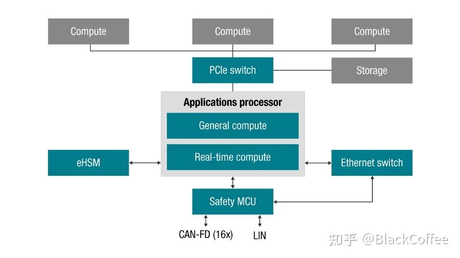
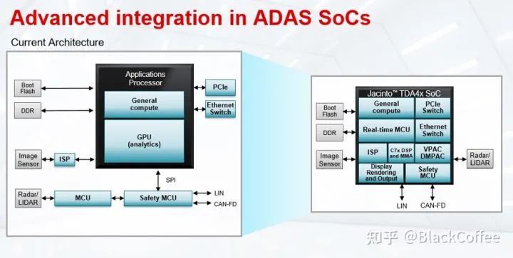
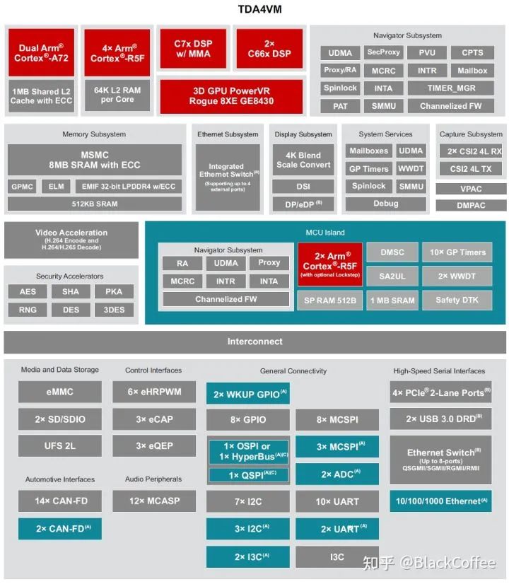
The TDA4VM processor based on the Jacinto™ 7 architecture is designed for L2+ level centralized ADAS domain controller platforms. It integrates various accelerators, deep learning processors, and on-chip memory, offering powerful data analysis and processing capabilities, making it a fully functional, programmable, high-integration ADAS domain control processor platform.This multi-level processing capability enables the TDA4VM to fulfill various roles as a central processing unit in the ADAS domain. For example, the TDA4VM processor supports the connection of 8MP (8 million pixels) high-resolution cameras, and stronger forward-looking cameras can help vehicles see further, thus enabling the development of stronger advanced driving assistance features. Users can also use the TDA4VM processor to operate 4 to 6 3MP cameras simultaneously, and it can also deeply fuse data from various sensors such as millimeter-wave radar, ultrasonic radar, and lidar on a single chip platform (post-fusion). The TDA4VM processor can also be used as the central processor in automatic parking systems, achieving 360-degree surround perception capabilities, thereby enabling the development of a better user experience 360-degree full-screen parking system.The left side of the following block diagram is the current typical ADAS system block diagram, where the main data processing part is completed by the GPU or NPU. Outside this application processor, MCU, external ISP, Ethernet switch, and PCIe switch are integrated. The right side shows the ADAS system block diagram after using the TDA4VM. The TDA4 integrates the aforementioned modules that were originally required externally into the chip, including the CPU for general processing, real-time MCU, functional safety MCU, C7x DSP, MMA deep learning accelerator, VPAC DMPAC vision accelerator, internal ISP, Ethernet switch, and PCIe switch, etc. Clearly, using TDA4VM can greatly simplify the hardware complexity of the ADAS system. TDA4x Domain Control Processor Simplifies ADAS System ArchitectureThe following diagram is the Block Diagram of the TDA4VM processor. The key features of its chip are as follows:1) It has two 64-bit Arm® Cortex®-A72 microprocessor subsystems, with a working frequency of up to 1.8GHz, 22K DMIPS;
Each Cortex®-A72 core integrates 32KB L1 D-Cache and 48KB L1 I-Cache.
Each dual-core Cortex-A72 Cluster shares a 1MB size L2 Cache.
2) There are six Arm® Cortex®-R5F MCUs, with a working frequency of up to 1.0GHz, 12K DMIPS;
Each core has 64K L2 RAM memory
The MCU subsystem in the isolated safety island has two Arm® Cortex®-R5F MCUs
The general computing part has four Arm® Cortex®-R5F MCUs
3) Two C66x floating point DSPs, with a working frequency of up to 1.35 GHz, 40 GFLOPS, 160 GOPS;4) C7x floating point, vector DSP, up to 1.0 GHz, 80 GFLOPS, 256 GOPS;5) Deep learning matrix multiplication accelerator (MMA), up to 8 TOPS (INT8) at 1.0GHz;6) Vision processing accelerator (VPAC) and image signal processor (ISP) and multiple perspective auxiliary accelerators;7) Depth and motion processing accelerator (DMPAC); TI TDA4x Processor Functional Module Diagram“C7x” is TI’s next-generation DSP, which integrates TI’s industry-leading DSP and EVE cores into a single higher-performance core while adding floating-point vector computing capabilities, thus achieving backward compatibility with old code and simplifying software programming. The new “MMA” deep learning accelerator can achieve up to 8TOPS of performance within the industry’s lowest power envelope. Dedicated ADAS/AV hardware accelerators can provide visual pre-processing as well as distance and motion processing.The TDA4VM processor also meets the overall system power consumption requirements well. When meeting the high-performance computing required for these ADAS domain controls, the TDA4VM processor requires only 5 to 20W of power, so active cooling is unnecessary. For example, Momenta had a demonstration at CES 2020, where customers touched the chip casing of the TDA4 and found that no heat dissipation was done on the chip casing, indicating that the power consumption is very low.The functional safety design in the TDA4VM processor includes two parts:1) The isolated functional safety island integrates two Cortex-R5F cores that support dual-core lockstep mode, achieving ASIL-D level functional safety;2) The remaining main processor part can achieve ASIL-B functional safety.
The isolated functional safety island integrates two Cortex-R5F cores that support dual-core lockstep mode, achieving ASIL-D level functional safety;
The two ARM Cortex-R5F cores in the functional safety island come with floating-point co-processors and support dual-core lockstep running mode.
512 bytes of Scratchpad RAM memory
Up to 1MB of on-chip SRAM with ECC support
Dedicated voltage and clock domains in the safety island (independent of the main processor)
Dedicated memory and interface design in the safety island (independent of the main processor)
The remaining part of the main processor can achieve ASIL-B functional safety:
On-chip memory and interconnects are ECC protected
Built-in self-test mechanism (BIST)
(2) DRA829V Gateway Chip
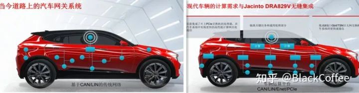
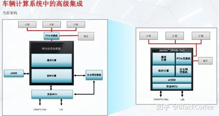
Traditional automobiles have been using low-speed networks (such as CAN/LIN, etc.) for communication, so if software upgrades are to be performed on all electronic control units of the vehicle, it will be very slow (as shown in the left part of the diagram below). When modern automobiles evolve to a domain-centralized EEA, such as the common three-domain EE architecture (ADAS domain, cockpit domain, vehicle control domain), high-speed communication buses are required between domains (as shown in the right part of the diagram below), thus requiring the central gateway’s network protocol conversion and packet forwarding capabilities. The DRA829V processor is designed for this scenario. DRA829V as the Communication Gateway between Automotive DomainsThe DRA829V processor is the industry’s first processor that integrates on-chip PCIe switches, and it also integrates an Ethernet switch that supports 8-port gigabit TSN, enabling faster high-performance computing and vehicle communication.The left side of the diagram below illustrates TI’s understanding of the entire vehicle computing platform framework. In this framework, external PCIe switches, Ethernet switches, and external information security modules (eHSM) and external MCUs need to be connected outside the application processor. The right side shows that with the DRA829V processor, all the aforementioned IP modules that were originally required externally are integrated, thus greatly reducing hardware complexity and improving reliability. The core aspect of TI’s automotive gateway processor is its high-performance processor while maintaining very low power consumption. TI DRV8x Series Gateway Chip Simplifies Gateway System ArchitectureThe DRA829V SoC addresses the challenges posed by the new vehicle computing architecture by providing computing resources, efficiently moving data within the vehicle computing platform, and facilitating communication across the vehicle network. It can be seen that the DRA829V mainly handles data exchange and security issues.Compared to NXP S32G2/S32G3, although both chips are designed for automotive central gateway scenarios, their design characteristics differ.
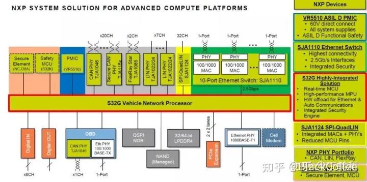
NXP S32G Central Gateway ProcessorNXP’s S32G is designed as a mature network processor, with the biggest feature being the acceleration of layer 3 protocol conversion and packet forwarding through a network offloading engine. It is entirely tailored for the central gateway scenario in the automotive domain centralized EE architecture and can effectively handle tasks such as OTA upgrades for various controllers, interaction of data gateways, and secure information transmission.On the other hand, DRA829V is more focused on the collection and forwarding of high-speed signals within the vehicle. These capabilities make DRA829V more suitable for acting as a high-speed signal collection and forwarding node within the domain (note: this is different from the central gateway role of NXP S32G, which can be considered as the gateway functionality required by the domain master control processor). Of course, DRA829V can also serve as a central gateway, but due to the lack of a packet forwarding engine similar to that in the NXP S32G gateway, this is not the main feature of DRA829V.
4. NVIDIA Xavier/Orin Solutions
NVIDIA is the world’s largest intelligent computing platform company. The company initially focused on PC graphics computing and later gradually expanded its business focus to AI acceleration in the cloud, high-performance computing (HPC), AR/VR, and other fields by leveraging its GPU architecture suitable for large-scale parallel computing. In addition to excellent hardware platform architecture and performance, NVIDIA also has a significant advantage in software and ecosystem. The CUDA software development platform based on NVIDIA GPU architecture is the industry standard for heterogeneous computing frameworks. NVIDIA has developed DNN acceleration libraries, compilers, development debugging tools, and TensorRT inference engines based on the CUDA computing framework.NVIDIA officially launched its intelligent processor Tegra X1 aimed at mobile, robotics, and autonomous driving fields in 2015, which integrated NVIDIA’s then most advanced Maxwell architecture GPU core. The release of this SoC processor also opened the AI computing era in the embedded field globally..Leveraging its accumulated advantages in the cloud with the CUDA+TensorRT ecosystem, NVIDIA provides an end-to-end solution in the autonomous driving field, including: Drive AV software platform, Drive IX software platform, Drive Sim, and a complete software ecosystem.
(1) Xavier Autonomous Driving Computing Platform
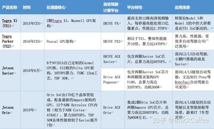
NVIDIA launched the Xavier platform at CES 2018 as an evolution of the Driver PX2. NVIDIA claims Xavier is the “world’s most powerful SoC (System on Chip),” capable of processing autonomous driving perception data from vehicle radar, cameras, lidar, and ultrasonic sensors, with a better energy efficiency ratio than similar products on the market and a smaller size. “NVIDIA® Jetson AGX Xavier™ sets a new benchmark for computing density, energy efficiency, and AI inference capabilities for edge devices.”The Xiaopeng P7, launched in April 2020, became the first mass-produced model equipped with the NVIDIA DRIVE AGX Xavier autonomous driving platform, featuring 13 cameras, 5 millimeter-wave radars, and 12 ultrasonic radars, integrated with the open NVIDIA DRIVE OS operating system.The Xavier SoC is based on TSMC’s 12nm FinFET process, integrating 9 billion transistors, with a chip area of 350 square millimeters. The CPU uses NVIDIA’s self-developed 8-core ARM64 architecture (codenamed Carmel), integrating a Volta architecture GPU (512 CUDA cores), supporting FP32/FP16/INT8. At 20W power consumption, it achieves single-precision floating-point performance of 1.3TFLOPS, with Tensor core performance of 20TOPs, and can reach 30TOPs when unlocked to 30W.Xavier is a highly heterogeneous SoC processor, integrating up to eight different processing cores or hardware acceleration units, allowing it to simultaneously and real-time process dozens of algorithms for sensor processing, ranging, positioning and mapping, vision and perception, as well as path planning tasks.
8-core CPU: Eight-core “Carmel” CPU based on ARMv8 ISA
Volta GPU: 512 CUDA cores | 20 TOPS (INT8) | 1.3 TFLOPS (FP32)
Vision Processor: 1.6 TOPS
Stereo and Optical Flow Engine (SOFE): 6 TOPS
Image Signal Processor (ISP): 1.5 Giga Pixels/s
Video Encoder: 1.2 GPix/s
Video Decoder: 1.8 GPix/s
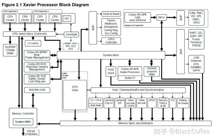
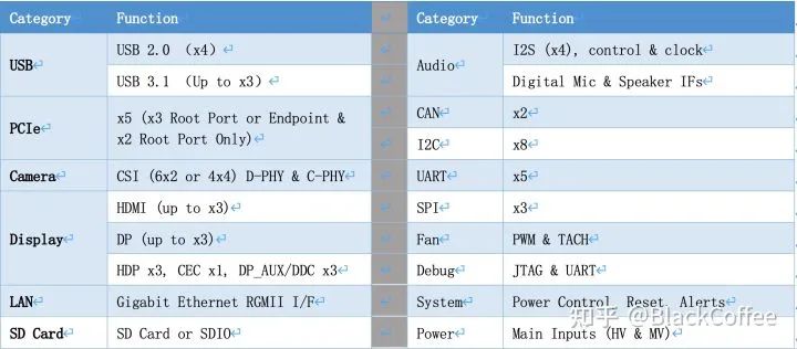
The main processor of Xavier can meet ASIL-B level functional safety requirements.Below is the Block Diagram of the Xavier SoC:NVIDIA Xavier Processor Functional Module DiagramIn addition to powerful computing resources, the Xavier SoC has a wealth of IO interface resources:Xavier has two versions of the system on module (SoM), namely Jetson AGX Xavier 8GB and Jetson AGX Xavier:
Jetson AGX Xavier 8GB: An affordable low-power version of the Jetson AGX Xavier, fully compatible with existing Jetson AGX Xavier in terms of software and hardware. The entire module consumes a maximum of 20W power while providing up to 20 TOPS of AI performance.
Jetson AGX Xavier: As the world’s first intelligent computing platform designed for autonomous robots, Jetson AGX Xavier can provide high computing performance while maintaining low power consumption. The Jetson AGX Xavier platform can preset three operating modes of 10W, 15W, and 30W, while the Jetson AGX Xavier Industrial version offers two optional power consumption modes: 20W and 40W.
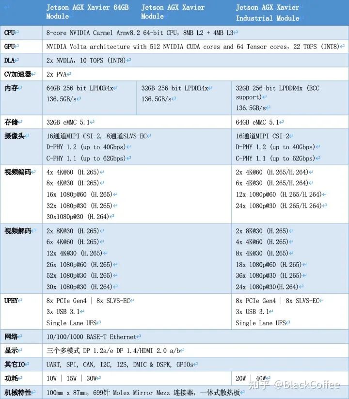
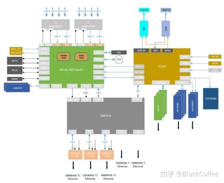
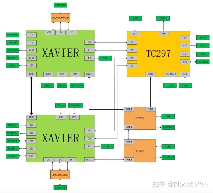
Below is the performance parameter comparison of different versions of the Jetson AGX Xavier system on module:Ecotron (ecotron.ai/) is a US manufacturer focused on ADAS DCU (ADCU). In September 2019, it launched the EAXVA03 ADAS domain controller, a high-performance central computing platform aimed at L3/L4 level autonomous driving, built using NVIDIA Xavier SoC and Infineon TC297 MCU. According to the design plan, the Xavier intelligent processor is used for environmental perception, image fusion, path planning, etc., while the TC297 MCU is used to meet ISO26262 functional safety requirements (ASIL-C/D level) in control application scenarios (i.e., as the Safety Core), such as safety monitoring, redundant control, gateway communication, and vehicle control.The latest models have developed to EAXVA04 and EAXVA05. EAXVA04 is an upgraded version of EAXVA03, still using one Xavier and one TC297 scheme, while EAXVA05 adopts a dual Xavier + TC297 scheme, thus providing greater computing power. Below is the structural diagram of the EAXVA04 ADAS domain controller: Structure Diagram of EAXVA04The following is the structural diagram of the EAXVA05 ADAS domain controller with dual Xavier + TC297 MCU: Structure Diagram of EAXVA05 ADAS Domain Controller
(2) Orin Autonomous Driving Computing Platform
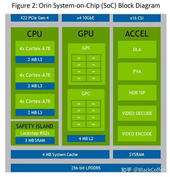
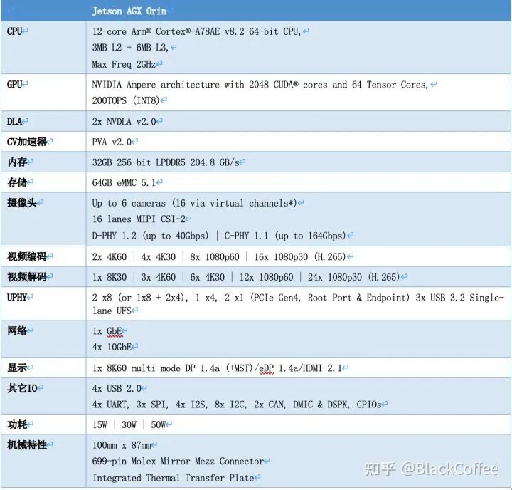
In December 2019, NVIDIA released the next-generation Orin chip and computing platform aimed at autonomous driving and robotics. It features ARM Hercules CPU cores and NVIDIA’s next-generation GPU architecture. The Orin SoC contains 17 billion transistors, nearly twice the number of transistors in the Xavier SoC, and has 12 ARM Hercules cores, integrating NVIDIA’s next-generation Ampere architecture GPU, providing 200 TOPS@INT8 performance, nearly 7 times that of the Xavier SoC. The Orin SOC will provide samples in 2021 and officially enter mass production for automakers in 2022.In May 2020, at GTC, NVIDIA introduced the upcoming next-generation autonomous driving Drive AGX Orin platform, which can carry two Orin SoCs and two NVIDIA Ampere GPUs, achieving a comprehensive performance enhancement from entry-level ADAS solutions to L5 autonomous taxi (Robotaxi) systems, with a maximum of 2000 TOPS computing power. Future L4/L5 level autonomous driving systems will require more complex and powerful autonomous driving software frameworks and algorithms. With its strong computing performance, the Orin computing platform will help concurrently run multiple autonomous driving applications and deep neural network model algorithms.As an intelligent computing platform designed specifically for autonomous driving, Orin can achieve ISO 26262 ASIL-D level functional safety standards.With the help of advanced 7nm process technology, Orin has excellent power consumption levels. At 200 TOPS of immense computing power, the TDP is only 50W.Below is the Block Diagram of the Orin SoC:NVIDIA Orin Processor Functional Module DiagramThe following table shows the performance parameters of the Jetson AGX Orin system on module:
On December 30, 2020, Great Wall Motors held a press conference to upgrade its intelligent driving strategy, officially launching the new Coffee Smart Driving “331 strategy.” At the conference, Great Wall also reached a strategic cooperation with Qualcomm to decide to equip mass-produced vehicles with the Qualcomm Snapdragon Ride autonomous driving platform. Great Wall Motors plans to launch the world’s first L4 mass-produced vehicle based on the Qualcomm Snapdragon Ride platform in 2022, equipped with IBEO’s 4D all-semiconductor true solid-state lidar, with an effective range of up to 300 meters.The Qualcomm Snapdragon Ride autonomous driving platform consists of two chips in terms of hardware:1) SA8540 main processor (serving as the main processor for ADAS domain applications, meeting system-level safety requirements);2) SA9000B accelerator, providing the computing power required for the autonomous driving system. Both achieve ASIL-D and can support L1~L5 level autonomous driving. The AI computing power of a single board is 360 TOPS (INT8), with an overall power consumption of 65 watts, and the computing energy efficiency ratio is about 5.5 TOPS/W. By using PCIe switches, it can be increased to 4 computing platforms, with a total AI computing power of 1440 TOPS from four accelerators.1) ADAS application processor: Kryo CPU, Adreno GPU, neural processor, embedded vision processor2) Autonomous driving dedicated accelerator (ASIC): neural network processor array
L1/L2 level ADAS: Targeting vehicles with driving assistance functions such as AEB, TSR, and LKA. Hardware support: 1 ADAS application processor, providing 30 TOPS of computing power
L2+ level ADAS: Targeting vehicles with HWA (highway assistance), automatic parking APA, and TJA (traffic jam assistance) functions. Required hardware support: 2 or more ADAS application processors, with expected computing power requirements of 60~125 TOPS
L4/L5 level autonomous driving: Targeting autonomous passenger cars, robot taxis, and robotic logistics vehicles in urban traffic environments; required hardware support: 2 ADAS application processors + 2 autonomous driving accelerators (ASIC), providing 700 TOPS of computing power, with a power consumption of 130W
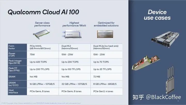
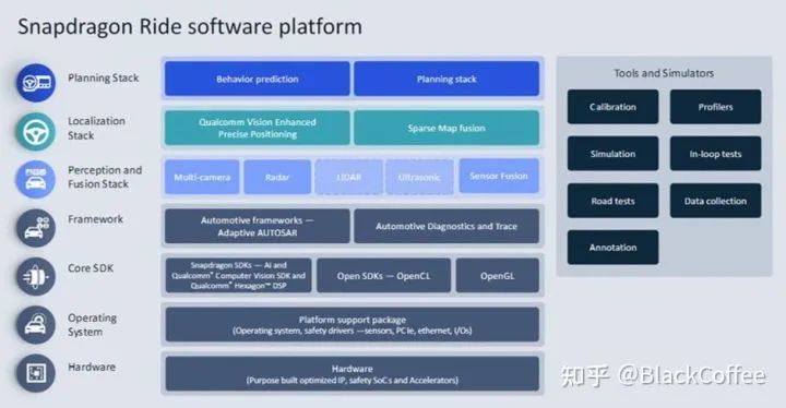
So far, Qualcomm has not disclosed information about its SA8540P and SA9000B chips. The likelihood of Qualcomm developing entirely new chips for L3/L4 autonomous driving is very low, so we can roughly infer from Qualcomm’s other related chip products. In the first half of 2021, Qualcomm officially commercialized an AI 100 edge computing suite, using Snapdragon 865 as the application processor and AI 100 as the accelerator, achieving 70 TOPS of computing power under the M.2 edge interface, and up to 400 TOPS under the PCIe interface with 16 cores.According to Great Wall’s promotional images, both 8540 and 9000 are 7nm, and both AI 100 and Snapdragon 865 are also 7nm. PCIe can also be seen in Great Wall’s promotional images. Of course, to meet automotive standards, some performance must be sacrificed, and power consumption must be reduced through frequency reduction, so performance is reduced to 360 TOPS. Snapdragon 865 is the top chip in Qualcomm’s 7nm line, and the frequency of 870 is even higher, reaching up to 3.2GHz, which will inevitably lead to higher power consumption, so 8540 is most likely a vehicle-grade version of Snapdragon 865, and of course, the X55 modem can be removed. Qualcomm only has one accelerator, and SA9000B is likely to be a vehicle-grade version of AI 100. Qualcomm Cloud A100 AI Acceleration ProcessorThe core of Qualcomm AI 100 follows the DSP route, with a maximum of 16 AI cores per chip. Each AI core has 9MB of SRAM, totaling 144MB for 16 cores, while Tesla’s FSD is 64MB, meaning AI 100 is basically twice that of Tesla. The Qualcomm suite uses 12GB of LPDDR5, while Tesla’s FSD can only correspond to LPDDR4.Of course, Qualcomm will not only provide hardware but will also offer a complete set of software and hardware solutions, including software SDKs, tools, and simulations. Qualcomm Snapdragon Ride Autonomous Driving Software Stack ArchitectureQualcomm’s partners for the autonomous driving platform focus on its visual perception and driving strategy software stack, Arriver. In fact, Arriver is Veoneer’s software brand, with Valeo primarily responsible for parking, and Park4u being the name of Valeo’s parking system. The primary partner for DMS is Seeing Machines, the supplier of DMS for Cadillac.Overall, Qualcomm’s strategy is to provide a complete end-to-end hardware and software solution while actively laying out corresponding ecological partners upstream and downstream.
6. Key Indicators of ADAS/AD Chips
As the brain of the entire vehicle, autonomous driving domain controllers typically need to connect multiple cameras, millimeter-wave radars, lidars, and IMUs, and process and compute the vast amounts of data from these sensor devices. Especially, the data volume generated by cameras and lidars is very large, thus requiring a core computing performance that is increasingly powerful for the autonomous driving main processor.Below we summarize the key indicators that autonomous driving main processors should have:(1) CPU CoresIn the automotive electronics field, the CPU core’s integer computing capability is usually measured in DMIPS (Dhrystone MIPS).The Dhrystone standard testing method is straightforward, running the Dhrystone program as many times as possible in a unit of time, with the metric unit being DMIPS/MHz. MIPS stands for Million Instructions Per Second, referring to the number of million-level machine language instructions processed per second. The D in DMIPS stands for Dhrystone, indicating the MIPS under the Dhrystone standard testing method.In addition to the Dhrystone Benchmark, CoreMark is another set of commonly used CPU core performance testing benchmarks in the embedded field. CoreMark was proposed in 2009 by Shay Gla-On from the Embedded Microprocessor Benchmark Consortium (EEMBC), primarily aimed at testing processor core performance, and this standard is considered to be more practically valuable than the outdated Dhrystone standard.(2) Memory BandwidthDue to the need to access large amounts of sensor data, the memory pressure on autonomous driving chip platforms is very high. The entire system often exhibits the characteristics of a Memory-Bound system, thus memory bandwidth usually determines the theoretical upper limit of system performance.For example, a common 256-bit LPDDR4@4266 has a bandwidth of: (256 * 4266) / (8 * 1000) = 136.5GB/s. A 256-bit LPDDR5@6400 has a bandwidth of: (256 * 6400) / (8 * 1000) = 204.8 GB/s.(3) AI Computing PowerAutonomous driving systems require significant computing power to process various sensor data, especially the processing of visual image data from cameras, which is the most computationally intensive.As the level of autonomous driving increases, the required computing power increases at least several times. For instance: L2 level requires more than 10 TOPS of computing power, L3 requires about 100 TOPS, L4 level might require around 500 TOPS, and L5 level might even require more than 1000 TOPS.Besides theoretical hardware computing power, the actual computing power utilization rate is also crucial. Different AI accelerator architecture designs typically lead to different actual utilization rates of hardware computing power, resulting in different measured performance of the same neural network model running on two AI accelerators with the same theoretical hardware computing power.(4) Energy Efficiency RatioThe energy efficiency ratio is the ratio of computing power to TDP power consumption, indicating the theoretical computing power value contributed per watt of power consumption, which is a very important indicator for measuring the quality of AI accelerator design. For example, the NVIDIA Orin chip has a computing power of 200TOPS and a TDP of 50W, resulting in an energy efficiency ratio of approximately 4TOPS/W.(5) Automotive Standards and Functional SafetyCompared to consumer electronics, automotive chips have the highest requirements for safety and reliability.Automotive chips operate year-round in harsh environments of “-40℃ to 125℃” high and low temperatures, as well as severe vibrations. To ensure that automotive electronic products meet high standards for operating temperature, reliability, and product lifespan, the Automotive Electronics Council (AEC) has established relevant quality certification standards, among which AEC-Q100 is the certification standard for stress testing of automotive integrated circuits. The AEC-Q100 standard has become the industrial standard for automotive electronic products in terms of reliability and product lifespan.In addition to meeting automotive-grade requirements, autonomous driving chips also need to meet the certification requirements for “Functional Safety” defined by the ISO 26262 standard. Functional safety imposes design requirements on chips to identify and correct failures as much as possible (divided into: systematic failures and random failures). Systematic failures are essentially design defects of the product, mainly relying on design and implementation process specifications to ensure, while random failures rely more on special failure detection mechanisms in chip design to ensure.ISO 26262 divides safety levels, commonly seen as ASIL-B and ASIL-D levels. ASIL-B requires that chips can cover 90% of single-point failure scenarios, while ASIL-D requires that it can reach 99%. The larger the chip area and the more transistors it has, the higher the corresponding failure rate.(6) Visual Interfaces and Processing CapabilitiesCameras currently typically use the MIPI-CSI2 interface standard for connection. MIPI CSI (Camera Serial Interface) is the interface standard designated by the MIPI Alliance’s Camera Working Group. CSI-2 is the second version of MIPI CSI, mainly consisting of application layer, protocol layer, and physical layer, supporting a maximum of 4-channel data transmission, with a single-wire transmission speed of up to 1Gb/s. The number of cameras that can be connected simultaneously is an important indicator of autonomous driving chips. For instance, NVIDIA’s Xavier/Orin allows for the simultaneous connection of 16 cameras.ISP, as the core chip for visual imaging processing, is also very important. Autonomous driving chips typically have integrated ISP modules. The raw image data from the camera sensor connected via the MIPI-CSI-2 interface is first sent to the ISP for processing, and the RGB/YUV image data processed by the ISP is then sent to other modules, such as CODEC or CV accelerators, etc. To achieve better image quality, the requirements for ISP in autonomous driving cars are very high.Moreover, other important features related to visual processing include: image rendering acceleration GPU, display output interfaces, and video codec.(7) Rich IO Interface ResourcesThe main control processor for autonomous driving needs a wealth of interfaces to connect various sensor devices. Currently, the common autonomous driving sensors in the industry include: cameras, lidars, millimeter-wave radars, ultrasonic radars, combined navigation, IMUs, and V2X modules.
The interface types for cameras mainly include: MIPI CSI-2, LVDS, FPD Link, etc.
Lidars are generally connected via standard Ethernet interfaces.
Millimeter-wave radars usually transmit data via CAN bus.
Ultrasonic radars are typically connected via LIN bus.
Combined navigation and inertial IMUs commonly use RS232 as their interface.
V2X modules also generally use Ethernet interfaces for data transmission.
In addition to the IO interfaces required for the aforementioned sensors, other common high-speed and low-speed interfaces are also needed, such as: PCIe, USB, I2C, SPI, RS232, etc.Welcome Angel Round and A Round Enterprises to Join the Group(Friendly connections include 500 automotive investment institutions including top-tier organizations; several enterprises have been successfully completed);There are communication groups for leaders of scientific and technological innovation companies,automotive manufacturing, automotive semiconductors, key components, new energy vehicles, intelligent connected vehicles, aftermarket, automotive investment, autonomous driving, vehicle networking, and dozens of other groups. To join, please scan the administrator’s WeChat(Please indicate your company name)