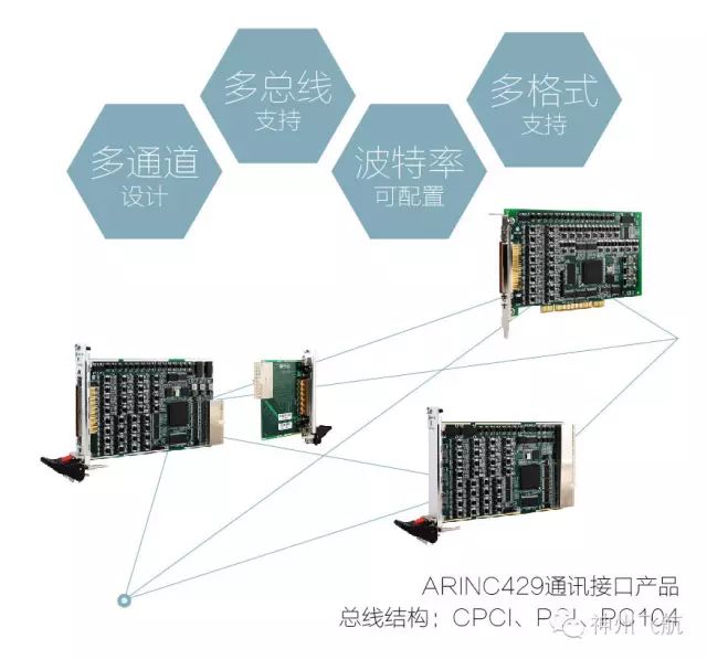
Introduction to ARINC429 Bus
>>>> Overview
-
The ARINC429 bus protocol was established by the Aeronautical Radio, Inc. (ARINC) and is a specification for civil aircraft onboard data bus.
-
The full name of ARINC429 is “Digital Information Transfer System”.
-
The ARINC429 bus is a serial standard designed for unidirectional broadcast transmission.
-
Only one transmitter is allowed on the bus, but it can have multiple receivers (up to 20).
-
Data is transmitted asynchronously using twisted pair shielded cable.
-
Transmission rates are divided into high and low: 100Kb/s and 12.5Kb/s.
>>>> Signal Characteristics
-
The ARINC429 data consists of 32-bit or 25-bit data with parity bits.
-
It uses a bipolar return-to-zero coding scheme (high, zero, low levels).
-
A signal returning from high to zero represents logic ‘1’, as shown in Figure A;
A signal returning from low to zero represents logic ‘0’, as shown in Figure B.
 >>>>Transmission Method
-
ARINC429 data uses differential transmission.
-
High-level voltage range is 4.5V to 5.5V, and low-level voltage range is -5.5V to -4.5V.
-
The waveform is as follows:
Positive terminal transmission
Negative terminal transmission

>>>>Data Features
-
The basic unit of ARINC429 data transmission is a word, consisting of 32 bits (or 25 bits).
-
Bit synchronization is achieved using bipolar return-to-zero coding.
-
Word synchronization is based on a time interval of at least 4 bits of zero level (word interval); the start of the first bit after this interval is the start of the new word.

-
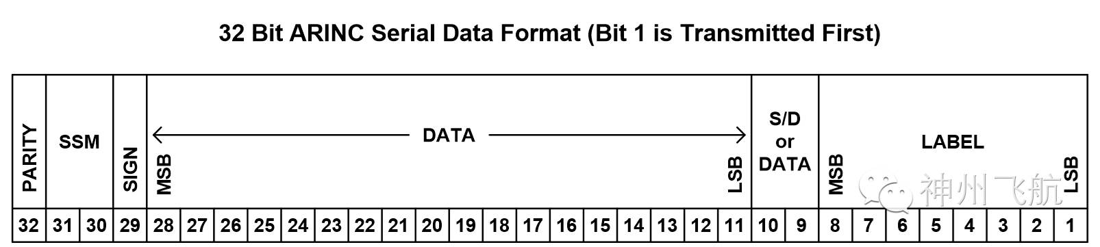
ARINC429 data words mainly consist of five parts: parity bit (P), sign status matrix bit (SSM), data bit (DATA), source/destination identifier (SDI), and label (LABEL).
-
The data transmission order starts from the first bit and sends sequentially to 32 bits (25 bits).
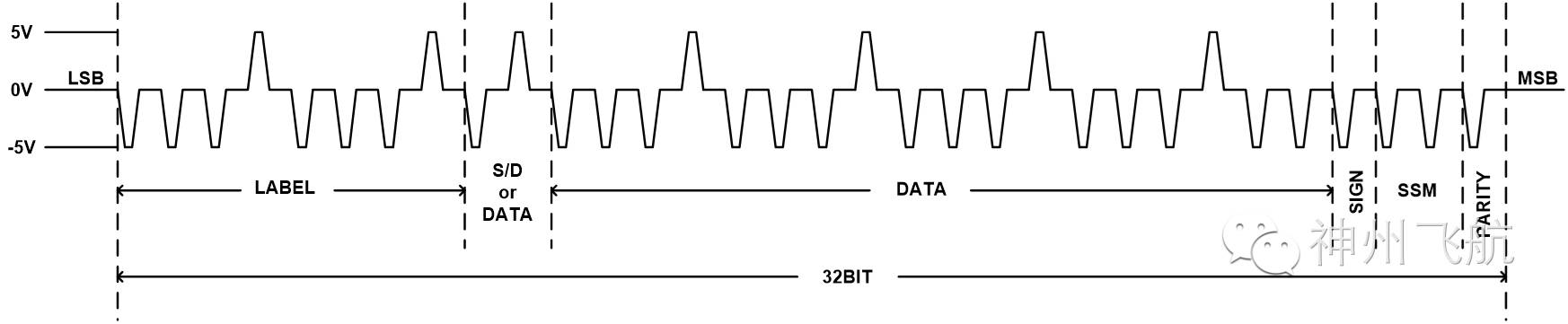
Data 0x11111111 odd parity waveform

>>>>Sending Odd Parity
-
Odd parityIn binary data, the total number of “1s” should be odd.
For other bits excluding the parity bit, if there is an odd number of “1s”, the parity bit is set to ‘0’; otherwise, it is set to ‘1’.
-
Even parityIn binary data, the total number of “1s” should be even.
For other bits excluding the parity bit, if there is an odd number of “1s”, the parity bit is set to ‘1’; otherwise, it is set to ‘0’.
-
ARINC429 sends the odd parity bit, taking 32-bit data as an example (the parity bit is the 32nd bit).
Odd parity:
If the lower 31 bits of the sent data have an odd number of ‘1s’, the parity bit is ‘0’; otherwise, it is ‘1’.
Even parity:
If the lower 31 bits of the sent data have an odd number of ‘1s’, the parity bit is ‘1’; otherwise, it is ‘0’.
When there is a parity check, the parity bit is modified according to the parity rule before sending; when there is no parity check, the data is sent directly without modification.
>>>>Receiving Odd Parity
-
Verification processFirst, receive the data containing the parity bit from the bus.Then, according to the receiving end’s parity check mode, check whether the received parity bit conforms to the parity rule.
If it conforms, the parity bit is set to ‘0’; otherwise, it is set to ‘1’.Finally, the parity bit is saved in the corresponding position.
-
ARINC429 receiving odd parity bit only indicates whether the verification result conforms to the receiving end’s parity rules.
If both the sending and receiving ends have parity checks and the parity methods are the same, a parity bit of ‘0’ in the received data indicates no parity error, while ‘1’ indicates a parity error.
If both the sending and receiving ends have parity checks and the parity methods are opposite, a parity bit of ‘1’ in the received data indicates no parity error, while ‘0’ indicates a parity error.
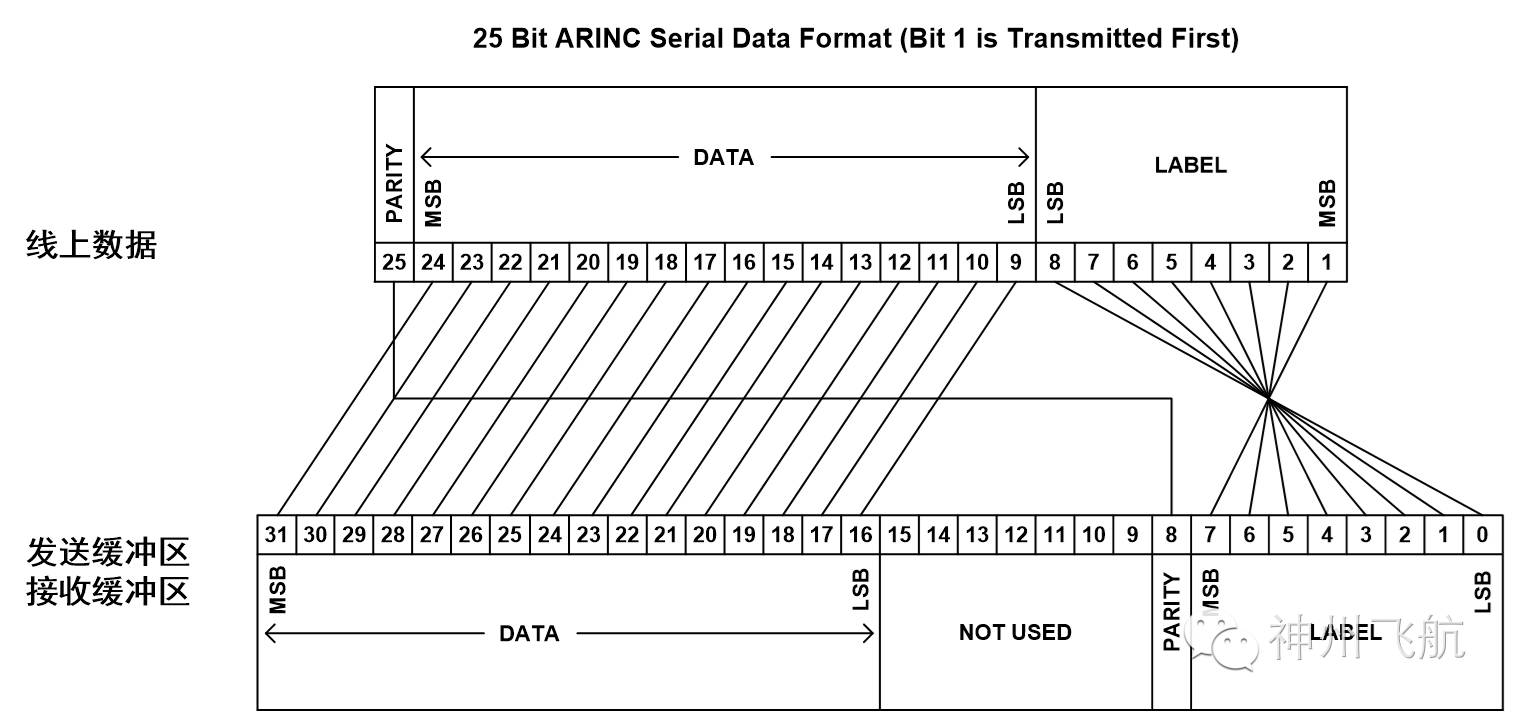
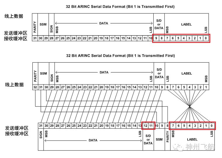
Data Format 1


Data Format 2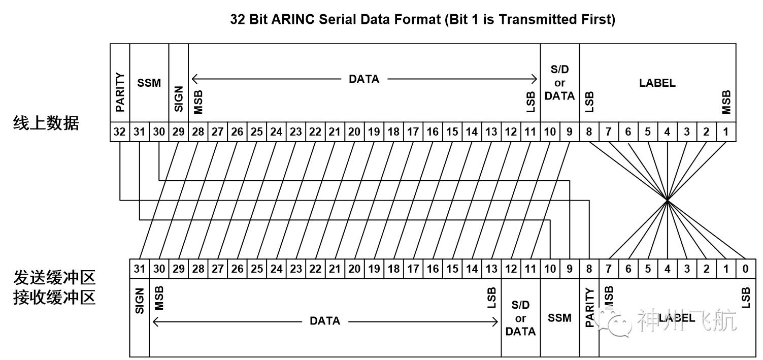
>>>>Receiving Data Filtering
-
Receiving data is filtered by setting the S/D number and label (LABEL).
-
Data that meets the filtering criteria will be received, while data that does not will be discarded.
-
Filtering is accomplished by setting the corresponding SD and label.
-
In the receiving label filtering settings, there are a total of 256 labels that can be set, with values ranging from 0 to 255; the S/D number can be selected from 0 to 3, allowing the card to filter up to 1024 different types of data.
-
When performing label filtering,
If the data format is Format 1, the label corresponds to bits 0 to 7 of the data, and the S/D number corresponds to bits 8 to 9 of the data.
If the data format is Format 2, the label corresponds to bits 0 to 7 of the data, and the S/D number corresponds to bits 11 to 12 of the data.
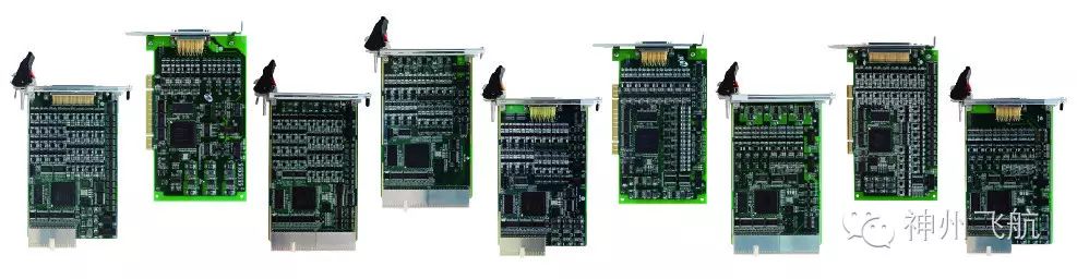
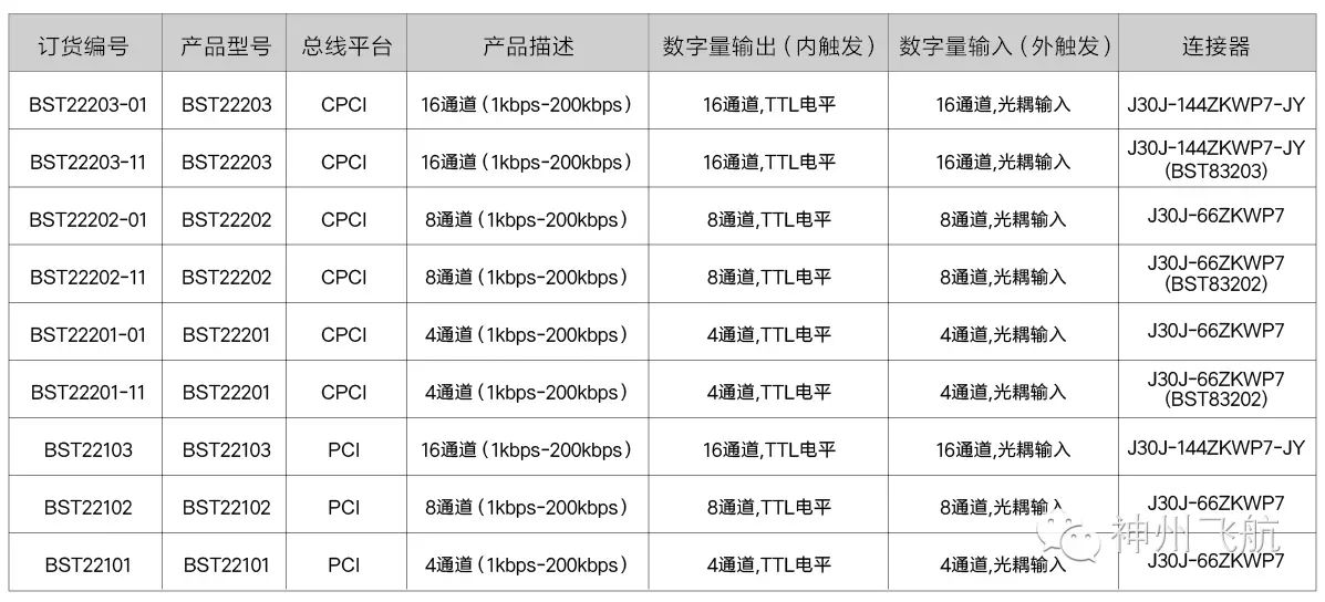
Product List
Glossary
-
Internal Trigger: A 50% duty cycle TTL square wave signal generated by the board itself, defining the frame interval for timed sending, with data transmission occurring at the valid edge of this synchronous clock.
-
External Trigger: A 50% duty cycle TTL square wave signal input from external devices via communication connectors, determining the frame interval for timed sending, with data transmission occurring at the valid edge of this synchronous clock.
-
Word Interval: The time interval from the end of the current ARINC429 word transmission to the start of the next ARINC429 word transmission, defaulting to 4 bits, which is the minimum achievable interval.
-
Timestamp: The time added to the received data word when the receiving end receives the data.
-
Label and S/D Filtering: Filtering based on the label information (the low 8 bits of the 429 word) and S/D number in the ARINC429 word; if it matches, the data is placed in the receive data buffer; otherwise, it is discarded.
-
Refresh Storage: Only stores the latest received data that meets the requirements; if reading is not timely, old data will be overwritten by new data.
Function Description
>>>>Sending Channel
-
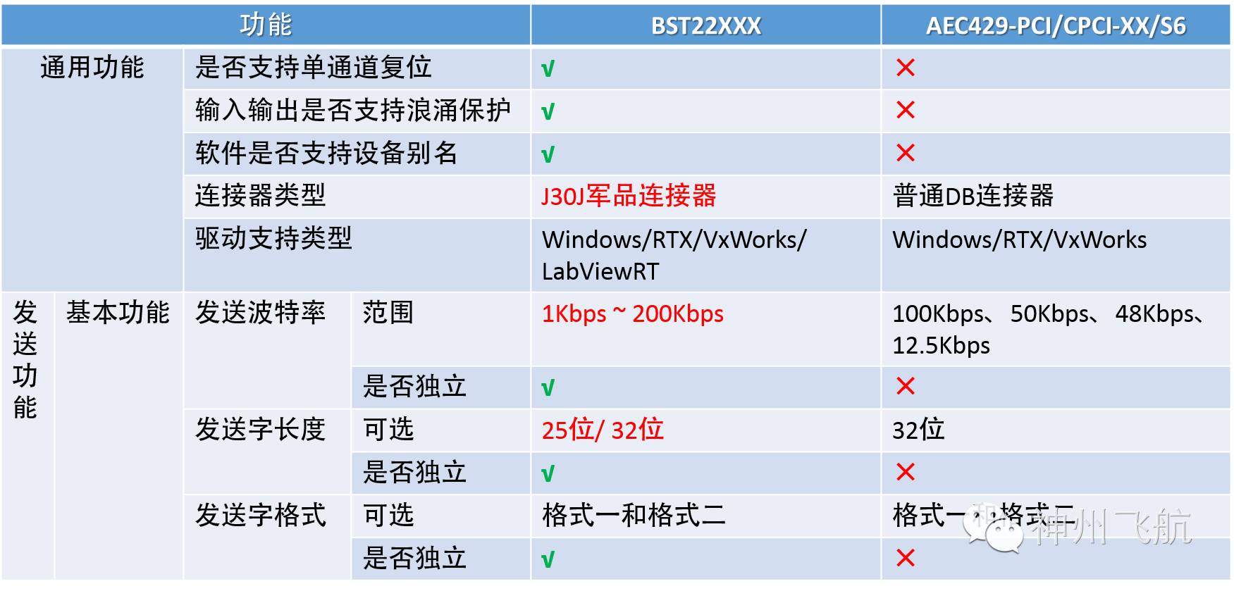
Each channel’s output port is surge protected.
-
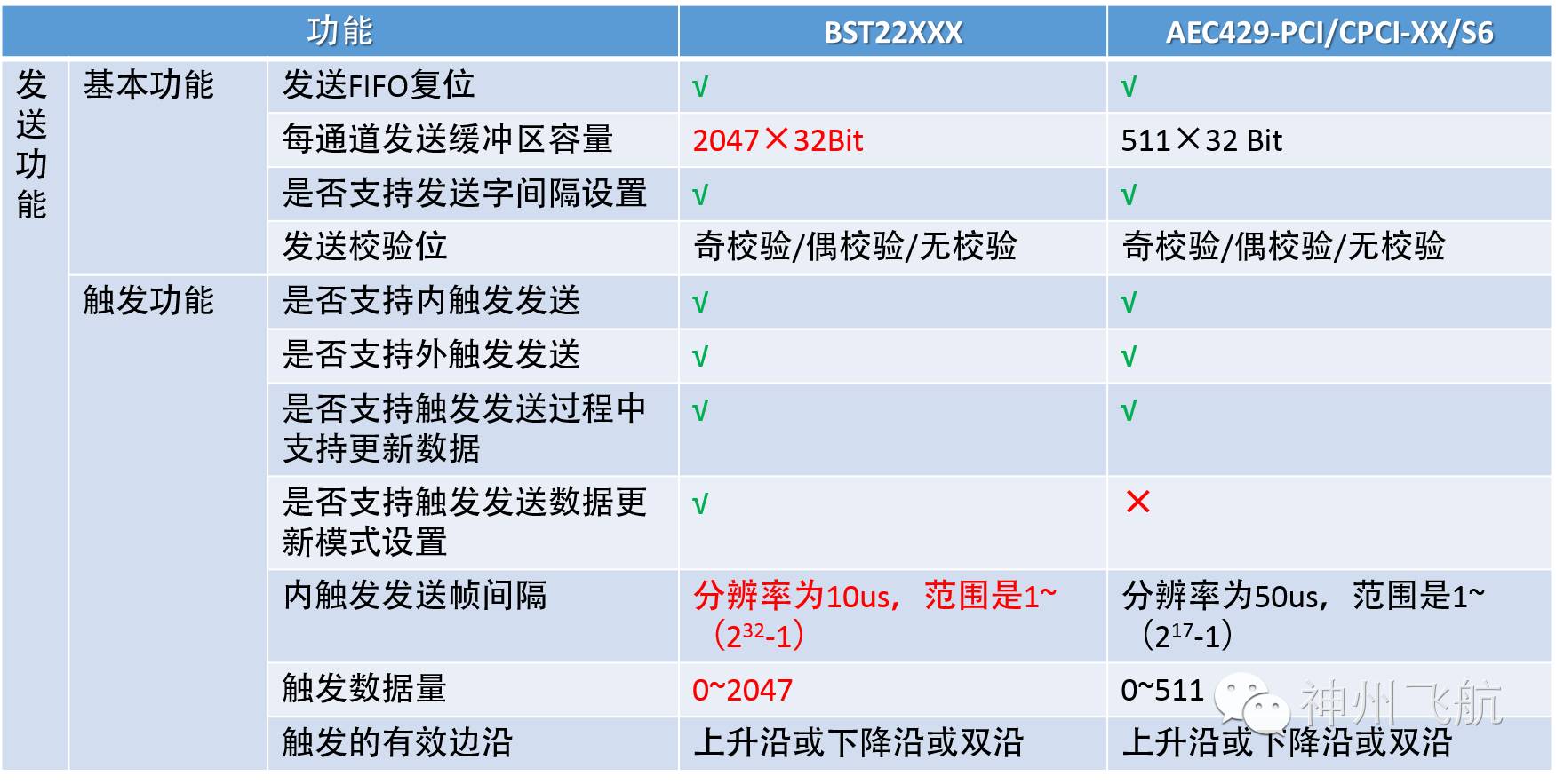
Each sending buffer has a capacity of 2047×32 bits.
-
The reset of each sending buffer can be controlled independently.
-
Sending baud rates support 100Kbps, 50Kbps, 48Kbps, 12.5Kbps, and user-defined rates.
User-defined baud rate range: 1Kbps to 200Kbps.
Sending baud rate can be set independently.
-
Sending word format can be set.
25 bits or 32 bits can be selected.
Supports odd parity/even parity/no parity.
Sending data supports two formats: Format 1 and Format 2.
-
Supports both internal and external trigger sending methods.
The number of timed sending times can be set by software, ranging from 0 to 65535.
The frame interval in internal trigger mode can be set by software, with a resolution of 10us, ranging from 1 to (2^31).
Word interval can be set by software, with a resolution of 0.5 bits, ranging from 8 to 65535.
The amount of trigger data can be set by software, ranging from 0 to 2047.
The valid edge of the trigger can be set to rising edge, falling edge, or both.
Data can be updated at any time during the triggering process.
>>>>Receiving Channel
-
Each channel’s output port is surge protected.
-
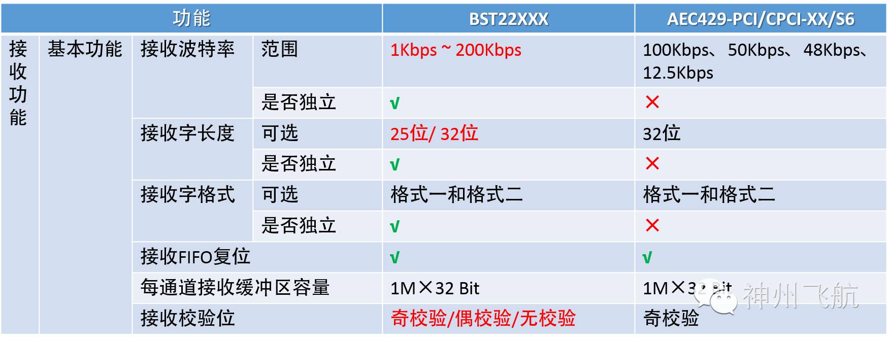
Each receiving buffer has a capacity of 1M×32 bits.
-
The reset of each receiving buffer can be controlled independently.
-
Each channel can independently control receiving enable.
-
Receiving baud rates support 100Kbps, 50Kbps, 48Kbps, 12.5Kbps, and user-defined rates.
User-defined baud rate range: 1Kbps to 200Kbps.
Receiving baud rate can be set independently.
-
Receiving word format can be set.
25 bits or 32 bits can be selected.
Supports odd parity/even parity/no parity.
Receiving data supports two formats: Format 1 and Format 2.
-
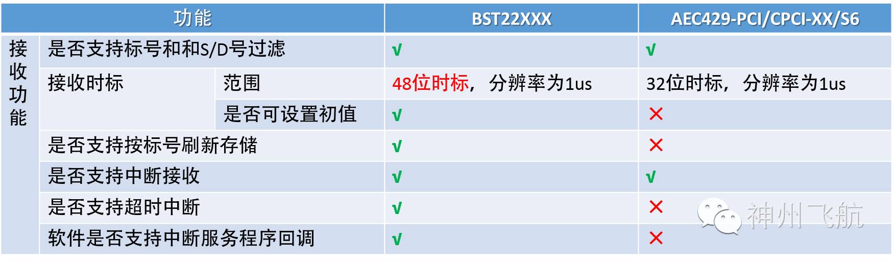
Supports receiving label and S/D number filtering functionality.
-
Each channel can independently control receiving enable.
-
Supports adding timestamps to received data.
Initial timestamp value can be set by software, with a 48-bit timestamp and a resolution of 1us, ranging from 1 to (2^48-1).
-
Receiving supports FIFO storage and refresh storage.
Refresh storage: supports storing the latest data by label.
-
Receiving trigger depth can be set.
-
Supports polling and interrupt receiving.
-
Supports timeout interrupts.
>>>>Trigger Function
-
Channel Configuration
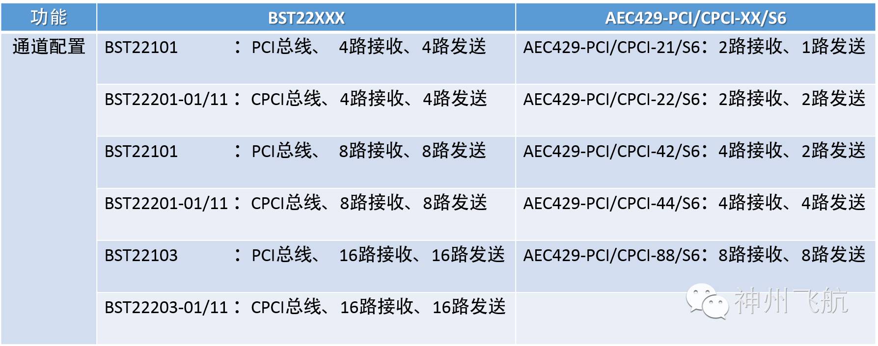
BST22101/BST22201: 4-channel trigger signal input/output.
BST22102/BST22202: 8-channel trigger signal input/output.
BST22103/BST22203: 16-channel trigger signal input/output.
-
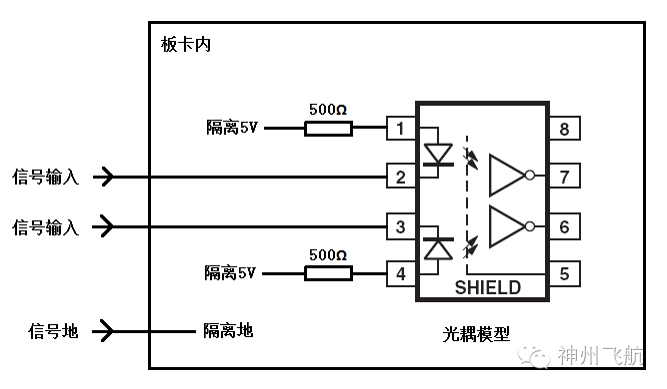
Trigger clock input signal: optocoupler input.
-
Trigger clock output signal: TTL output.
-
Trigger clock input signal is used for external trigger mode.
-
Trigger clock output signal is used for internal trigger mode.
>>>>Trigger Input Channel Signal Connection
-
Trigger clock input signal is optocoupler input.
-
The forward working current IF required for the optocoupler is between 5mA and 15mA.
Function Comparison
Application Usage
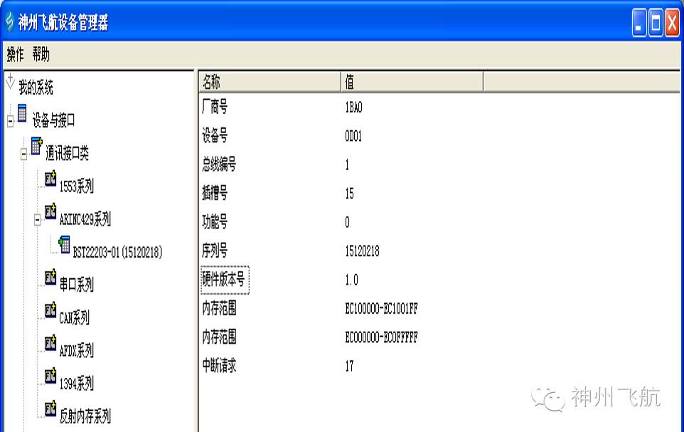
>>>>Device Manager
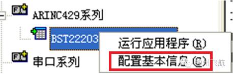
>>>>Setting Device Alias
Right-click
Uniqueness
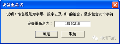
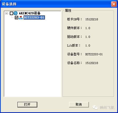
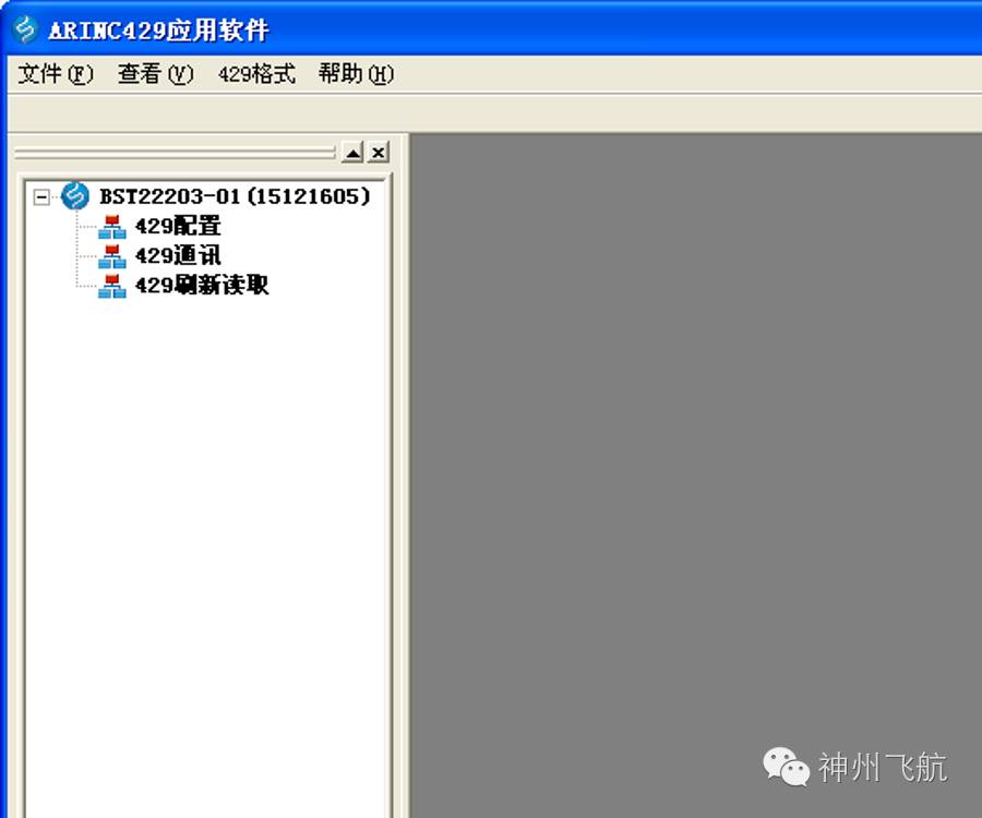
>>>>Device Selection and Function Selection
>>>>Configuration Interface
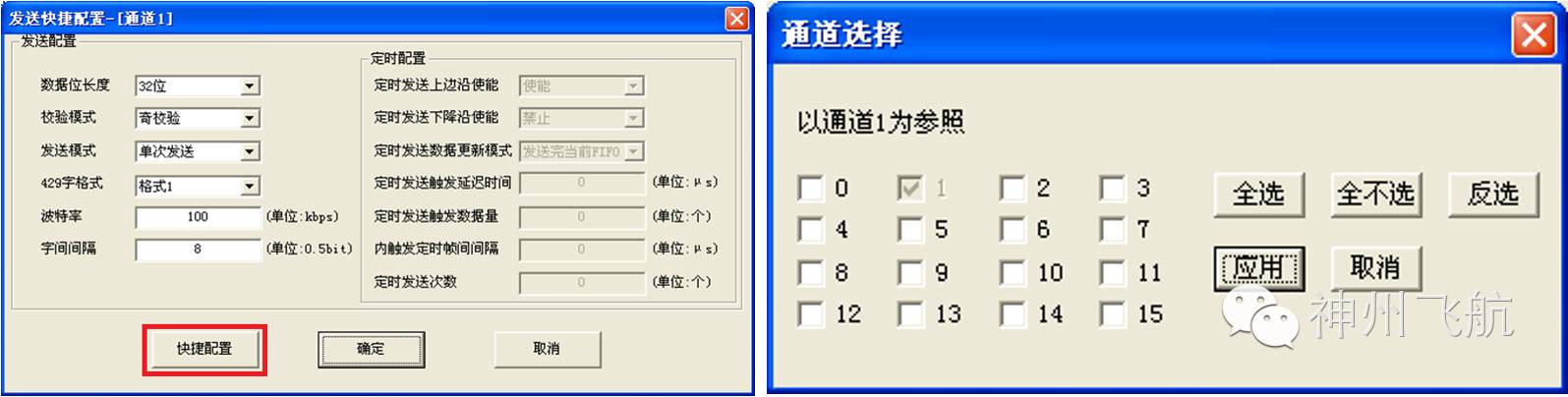
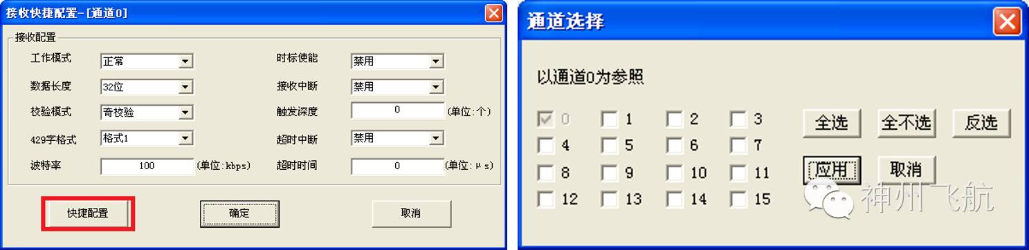
Click on the channel number to enter quick configuration.
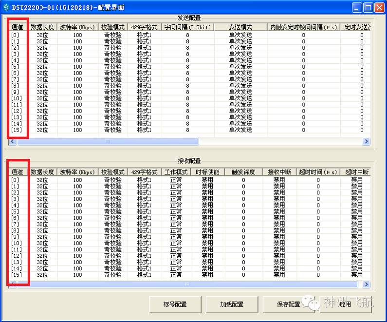
>>>>Sending Configuration Interface
>>>>Receiving Configuration Interface
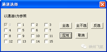
>>>>Communication Interface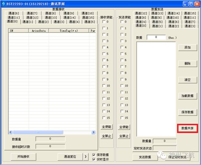
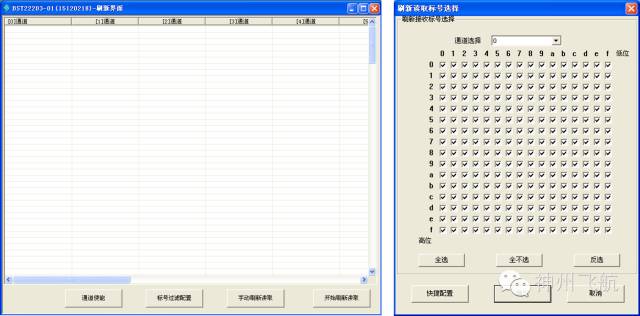
>>>>Refresh Interface
For more details, please visit the company website: www.senfetech.com