
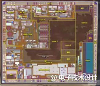
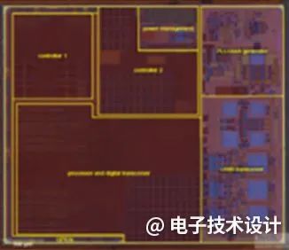
The sizes of the two chips are similar, and both are manufactured by TSMC, but there are significant differences. For example, the UWB transceiver and power management of the SR040 occupy 45% of the die area, while Apple’s U1 only occupies 33%. In terms of processor and memory, the SR040 occupies 37%, while Apple’s U1 occupies 57%. The process technology of the SR040 is 40 nm, formed by 8 metal layers, while Apple U1’s process technology is 16 nm, formed by 13 metal layers.Recently, Techinsight compared the teardown of Samsung SmartTag+ and Apple AirTag in a blog post, focusing on the performance comparison of the UWB devices used (NXP’s SR040 and Apple’s U1 TMKA75).Here are the results:
 |
 |
|
| Manufacturer | NXP SR040 | Apple U1 (TMKA75) |
| Die Size (Seal) | 3.09 x 3.33 (10.29 mm2) | 2.97 x 3.27 (9.71 mm2) |
| UWB Transceiver and PLL (mm 2 as % of die) | 1.8 mm2 – 18% | 2.8 mm2 – 29% |
| Power Management (mm2– as % of die) | 2.7 mm2 – 27% | 0.4 mm2 – 4% |
| Power Core and Embedded Memory (mm2– as % of die) | 3.6 mm2 – 37% | 5.5 mm2 – 57% |
| Foundry and Process | TSMC, 40 nm CMOS | TSMC, 16nm FinFET |
| Number of Metal Layers | 8 (7 copper, 1 aluminum) | 13 (12 copper, 1 aluminum) |
As we can see, the sizes of the two chips are similar, and both are manufactured by TSMC, but there are significant differences. For example, the UWB transceiver and power management of the SR040 occupy 45% of the die area, while Apple’s U1 only occupies 33%. In terms of processor and memory, the SR040 occupies 37%, while Apple’s U1 occupies 57%. The process technology of the SR040 is 40 nm, formed by 8 metal layers, while Apple U1’s process technology is 16 nm, formed by 13 metal layers.Here are the specific product teardowns:Samsung EI-T7300 (SmartTag+)
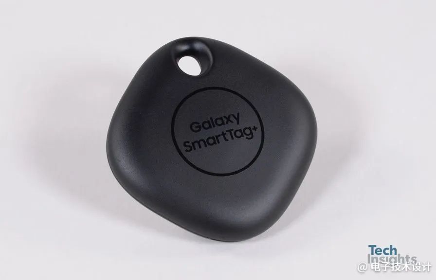 Figure 1. Samsung EI-T7300 (SmartTag+)
The Samsung EI-T7300 (SmartTag+) uses NXP’s SR040 UWB transceiver processor chip. The NXP Semiconductor SR040 uses a QFN package, which consists of a single die bonded to a lead frame. The key dimensions measured and the observed transistor characteristics indicate that the SR040 chip uses TSMC’s 40 nm CMOS process.
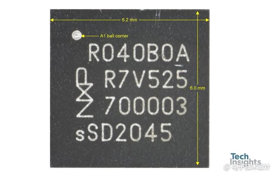 Figure 2. NXP Semiconductor SR040
The SR040 chip consists of a UWB analog front-end transceiver, several power management circuits, several SRAM memories, an ARM Cortex CPU, and several GPIOs.
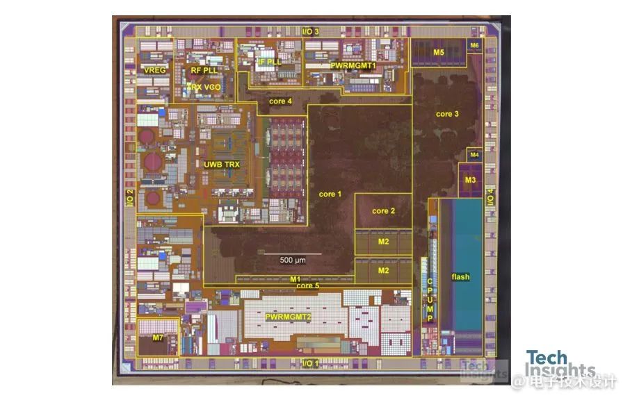 Figure 3. NXP Semiconductor SR040 Chip Photo
Let us take a deeper look at the UWB analog front-end transceiver.
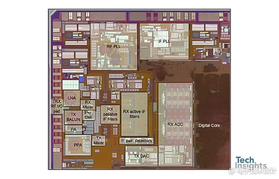 Figure 4. UWB Analog Front-End Transceiver
The UWB transceiver macrocircuit can be divided into two halves. In the lower half, we find the RF signal path, while the RF and IF PLLs are in the upper half. A shared RF pad connects the receiver and transmitter.The receive path includes an LNA with input matching circuitry, RX quadrature down-conversion mixer, a pair of passive filters, and a pair of active filters consisting of two second-order stages, and finally a pair of time-interleaved ADCs, each including a successive approximation sub-ADC.The transmit lineup includes a TX DAC formed by two cascaded sub-DACs, an up-conversion TX mixer, a power amplifier, and a BALUN transformer.The RF PLL includes the same LC resonant circuit-based oscillator. The quadrature phase required by the receiver is generated near the oscillator and sent to their destinations using differential coplanar transmission lines. The transmitter uses one of the same two phases. Since the IF portion of the transmitter is not quadrature, phase modulation must be generated in the RF PLL and applied to the signal in the mixer. The clocks for the RX ADC and TX DAC are generated in the IF PLL, which includes a three-stage differential CMOS ring oscillator.
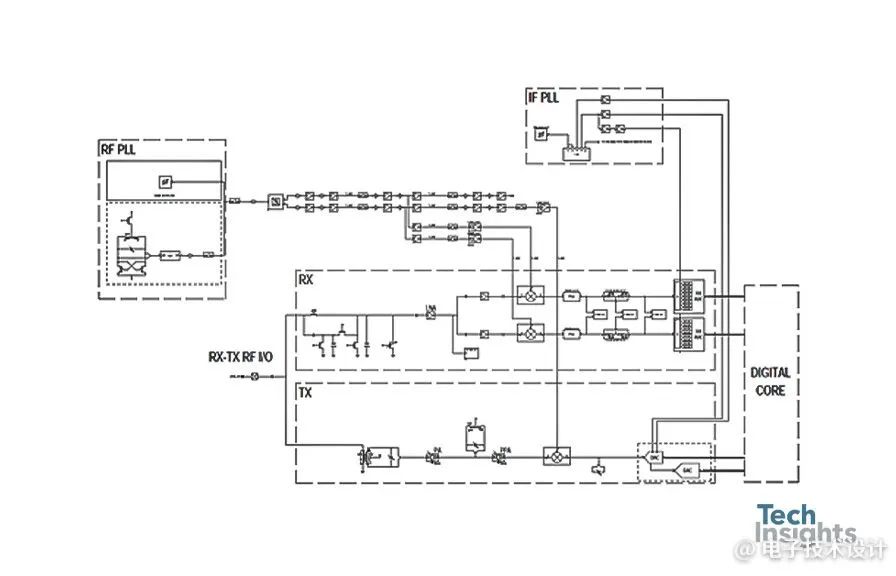 Figure 5. Circuit Analysis
Apple AirTag
UWB is not a new concept for Apple. They applied for a patent for “Ultra-wideband radio for time-of-flight ranging and network location estimation” in 2006 and have since applied for at least three related patents. The above is a brief summary of two devices that use the UWB communication standard for object tracking.A device the size of a quarter can have multiple antennas, a radio IC, a battery, and can continue to operate as a two-way radio, accurately locating objects within a few feet for nearly an entire year.
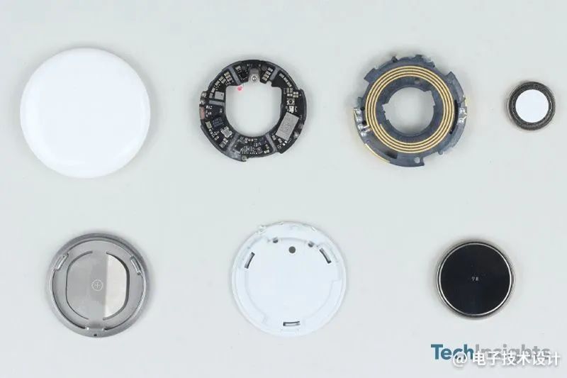 Figure 1. Apple AirTag Main Components
Apple AirTag is equipped with the Nordic nRF52832, which is manufactured using a 90nm process node, an improvement over the 180nm process used in slightly older 2.4 GHz Nordic transceiver ICs. The nRF52832 in the AirTag is in a WLCSP50 package, which is 75% smaller than the larger 48-pin 6 mm x 6 mm QFN option. There could be various reasons for choosing the WLCSP50 over the QFN package, one of which might simply be requiring less PCB space to utilize the multifunctional Nordic chip.
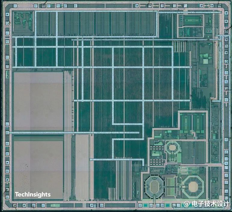 Figure 2. Nordic nRF52832 Chip Photo
Apple U1 UWB SIP (System in Package) – contains the Apple UWB transceiver, embedded crystal oscillator, Sony RF switch, and smaller discrete components in a single package with a total package area of 20.58 mm2.
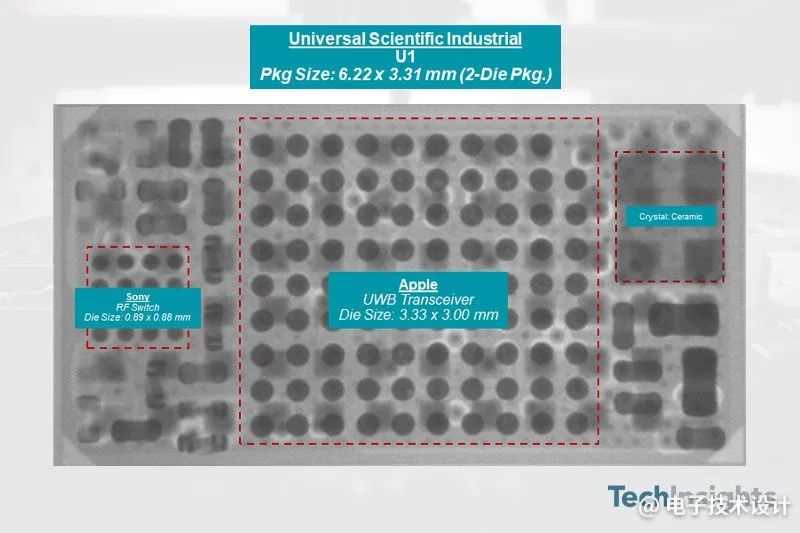 Figure 3. Apple U1 UWB SiP
The radio IC of Apple AirTag occupies less than 30mm2 or 6% of the total available PCB area. However, the performance of the AirTag, i.e., its success in staying connected to the Find My network, relies not only on the radio IC but also largely on its antenna and antenna design.However, the small size of the AirTag does not allow for separate antenna components as seen in other larger devices (such as phones). Instead, the AirTag has a framework that designs all three antennas.
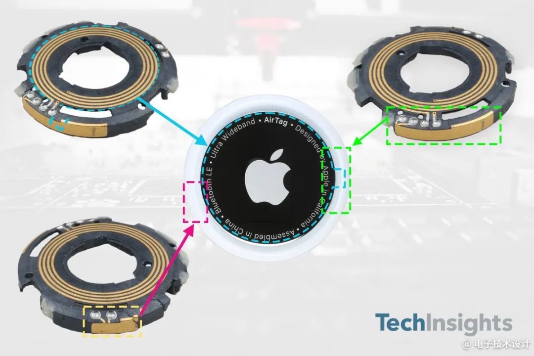 Figure 4. Apple AirTag Antenna Design
Apple has also included a speaker in the AirTag, which can emit a “chirp” sound for various scenarios. The Maxim class D audio amplifier located on the PCB drives the speaker.It’s worth noting not only the functionality and design of the AirTag. The retail price of the AirTag is less than $30, with an estimated manufacturing cost of $10 (excluding software costs and R&D). Tracking devices are not new, and Apple is not the first company to offer such products. Today, we are still in the early stages of UWB-based technology development, needing to address issues such as data privacy and efficiency, currently only used for replacing car keys or finding my wallet, but what about future use cases? It is worth looking forward to.END♥Click 👇 the business card to follow me♥Previous Recommendations1. A very clever automatic switching circuit for main and auxiliary power, with “zero” voltage drop, have you learned it? 2. Input and output impedance, how does it work? Do you know? 3. The ultimate secret of DCDC layout