1. Introduction to CoreSight
CoreSight is a new debugging architecture launched by ARM in 2004, designed for debugging and tracing complex SoC implementations.
A variety of CoreSight components make up a CoreSight system. CoreSight products include various tracing macro units for ARM processors, system and software measurement, and a complete set of IP blocks for debugging and tracing complex multi-core SoCs.
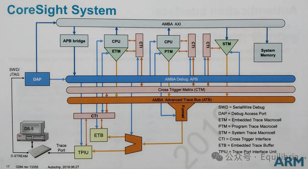
The above image shows a typical CoreSight architecture, which includes three pathways:
- Debug Pathway: Implements online debugging and simulation functions for external debuggers to debug the ARM core. The DAP receives SWD/JTAG data from external ports, converts it into access to the internal AP of the DAP, and then the AP converts it into memory-mapped bus access to access internal chip resources.
- Trace Pathway: Collects information about program execution The tracing interface allows debuggers to collect information about program execution while the program is running. The collected information can be the program instruction stream information generated by the Embedded Trace Macrocell (ETM) (instruction tracing), data/event/performance analysis information generated by the Data Watchpoint and Trace (DWT), or information generated by the Instrumentation Trace Macrocell (ITM).
- Trigger Pathway: Used to pass a debugging event from one processor to another This is used to send trigger signals to specified components or receive trigger signals from specified components. This function is implemented by the CTI and CTM. Each core is connected to a CTI component, which can send trigger signals to the processor or receive trigger signals from the processor.
2. CSS-600 and CSS-400
Both are solutions provided by ARM for chip debugging and tracing, with CoreSight SoC-600 being ARM’s next-generation debugging and tracing tool.CSS-600 is a pitfall, the biggest problem is that it is not backward compatible with CSS-400! The content described below is based on CSS-400.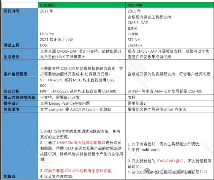
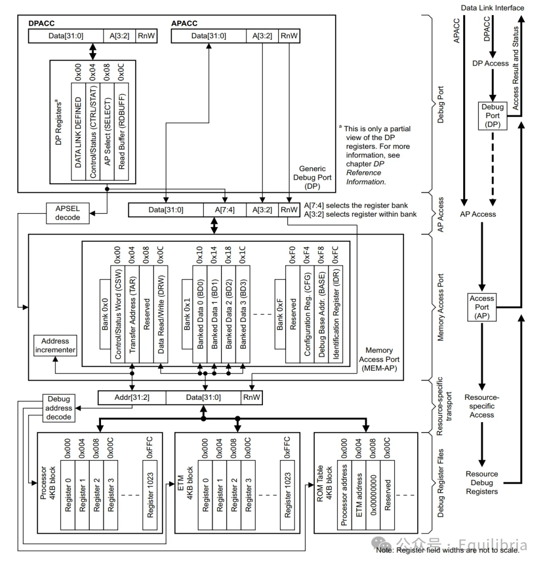
3. Debug Access Port
Although the DAP is not a component of CoreSight, it is used to access CoreSight components.
The DAP includes the following:
- APB Access Port (APB-AP)
- AHB Access Port (AHB-AP)
- AXI Access Port (AXI-AP)
- JTAG Access Port (JTAG-AP)
- Serial Wire JTAG Debug Port (SWJ-DP)
- JTAG Debug Port (JTAG-DP)
The DAP mainly consists of a DP and AP.
The DP receives JTAG or SW data sent by the external debugger, converting it into access to the internal AP. After passing through the decoder module, it determines which AP to access and sends the access information to the corresponding AP.
After the AP receives access from the DP, it converts it into the corresponding bus access to access internal resources. The access information is then sent back to the DP, which returns the access information to the debugger via JTAG or SW.
Each access by the emulator to the chip consists of a Transfer Request and Transfer Data.
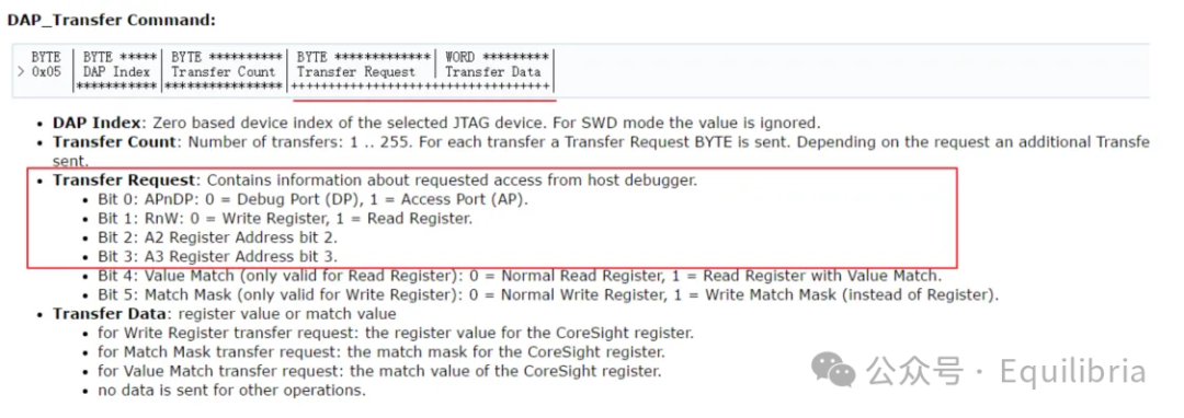
Bit0 is used to confirm whether the access is to the DP or AP, and Bit1 selects read or write.
After confirming the selection of the AP port, the next step is to confirm which register of the AP to select. The A[7:4] in the figure is used to determine which bank of the AP register to access through the DP port.
Then, based on A[3:2], it confirms which register to select. In Bank 0, we use two registers.
The first is the TAR register, with an address of 0x04. The function of this register is to write the address of the desired chip core register to access, and the AP port will access the corresponding core register at this address. The DRW register’s function is for the AP port to write the value of DRW into the register corresponding to TAR or read the value of the register corresponding to TAR into DRW.
For example: first send the control word 0x05 (select AP port, write operation, select TAR register), then send the address 0XE000ED0C, followed by control word 0x0D (AP, write operation, select DRW register), and finally send data 0X05FA0004, thus achieving the reset function.
4. ROM Table
In a SoC, there are multiple CoreSight components, but how does the software identify these CoreSight components and obtain information about them?
This relies on an important component within the CoreSight components: the ROM table.
ARM specifies that at least one ROM table must be implemented in a SoC, which stores information about the various CoreSight components in the SoC, including component formats and base addresses. The ROM table occupies only a 4K space, meaning the size of the PIDR4 register is 0.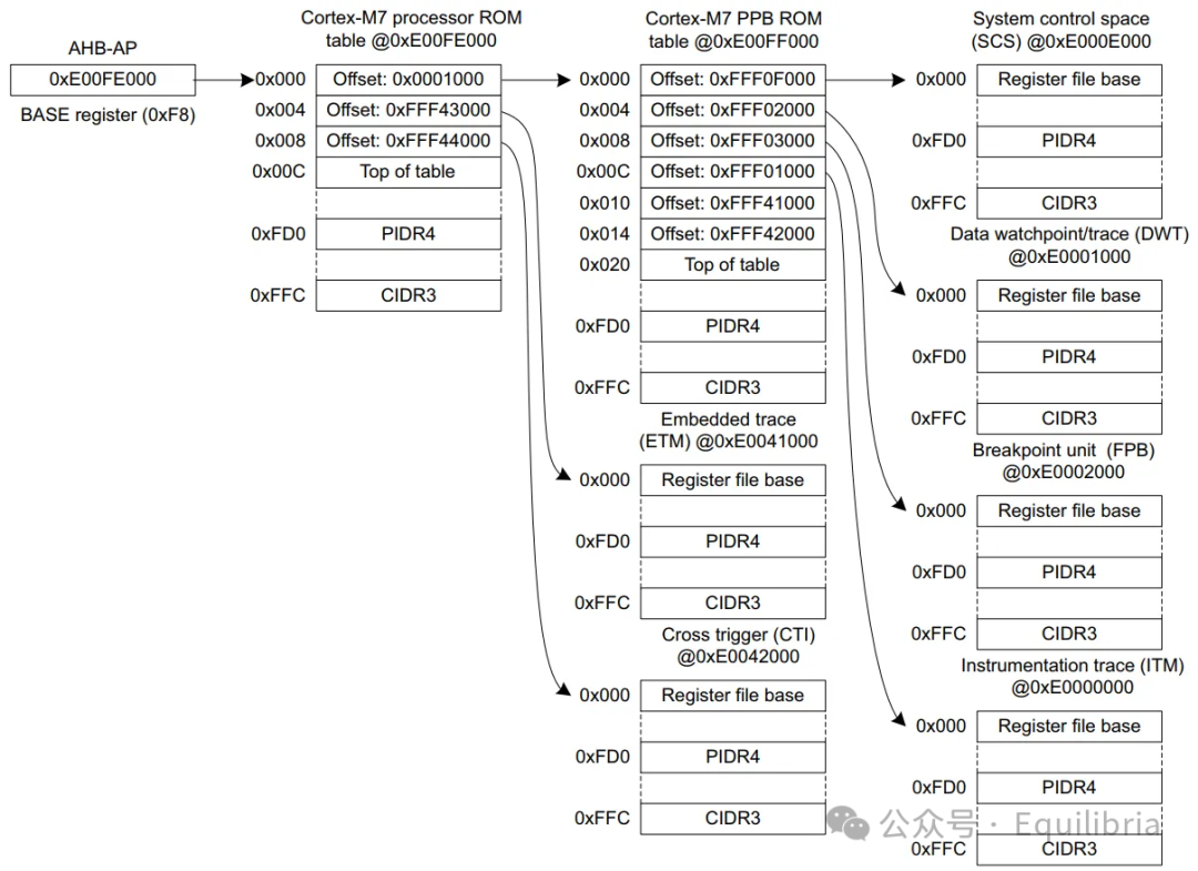
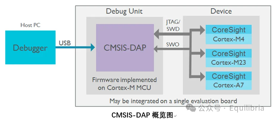
5. CMSIS-DAP
CMSIS-DAP is a firmware implementation and specification that supports access to CoreSight DAP, simply understood as a standard software debugging access interface launched by ARM.
CMSIS-DAP supports target devices that include one or more Cortex processors, providing a debug access port (DAP), typically using a 5-pin JTAG or 2-pin Serial Wire Debug (SWD) interface.
CMSIS-DAP connects the debug port to the USB debug unit’s interface firmware, allowing the debugger running on the host to connect to the target device running the application via USB.
For detailed reference:
- DAPLink Software Address
https://github.com/ARMmbed/DAPLink
- DAPLink Hardware Address
https://github.com/ARMmbed/mbed-HDK-Eagle-Projects
6. Debug Functions
- Access control registers for debugging and tracing features
- Step, stop, and reset program control
- Insert/remove breakpoints
- Access memory space. Memory space access can also be performed while the processor is running
- Access processor core registers. This can only be operated when the processor is stopped
- Flash programming
7. Trace Functions
The tracing interface allows debuggers to collect information about program execution in real-time while the program is running, providing many useful insights without needing to stop the processor.
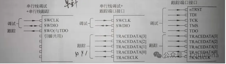
There are two types of tracing interfaces available:
- Serial Wire Viewer (SWV) – A single-pin line tracing interface that can selectively support data tracing, event tracing, performance analysis, and measurement tracing.
- Trace Port – Multiple data lines plus a clock signal line. It has a wider tracing bandwidth than SWV and can support all tracing types of SWV plus instruction tracing. On Cortex-M3/M4 devices, the trace port typically has four data lines and one clock line.
The trace port interface provides greater trace data bandwidth, but requires a more complex and expensive trace adapter to capture trace information using the trace port interface.
The trace port provides the following functions:
- Data tracing: Information about memory addresses (e.g., a combination of address, data, and timestamp) can be collected when the processor accesses this address
- Performance analysis tracing: The number of clock cycles used by the CPU for different operational tasks (e.g., memory access, sleep)
- Event tracing: Provides runtime and historical data of processor responses to interrupts/exceptions
Instruction Trace Macrocell (ITM)
ITM has multiple functions:
- Software tracing. Messages can be written to the ITM stimulus port register, and ITM will place the data in trace packets and output them through the trace interface.
- Trace packet merging. It merges trace packets generated by DWT, stimulus ports, and timestamp generators
It generates timestamp packets inserted into the trace stream, which can help the debugger reconstruct the timing information of events.
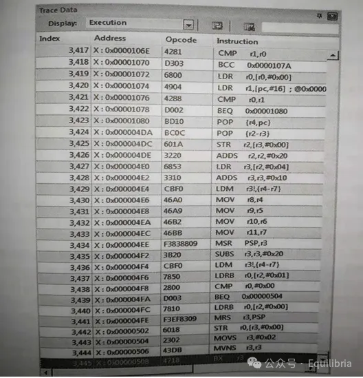
Embedded Trace Macrocell (ETM)
ETM is used for instruction tracing (optional IP, some chips do not provide this function). Once enabled and tracing begins, it generates instruction trace packets.
To reduce the amount of data generated by ETM, it does not always output the addresses executed by the processor; it generally outputs information about the program flow and only outputs the full address when necessary.
Micro Trace Buffer (MTB)
When a program execution fails and the processor enters HardFault, the instruction execution history and the program executed before the error event are very helpful. This feature is implemented by instruction tracing, and is one of the important reasons for adding MTB in the Cortex-M0+ processor.
MTB is a small component located between SRAM and the system bus. In normal operation, the role of MTB is to connect on-chip SRAM to the AHB interface module. During debugging operations, the debugger can configure MTB to use a small portion of SRAM as a trace buffer to store trace information.
When a program jump occurs, or the program flow changes due to an interrupt, MTB will store the source program counter and destination program counter into SRAM. During debugging pauses, the SRAM data can be extracted, and the Trace window can show the instruction execution status from running to stopping during that time.
8. ResetReset
For typical Cortex-M processors, there are three types of resets:
Power-on Reset: Resets all parts, including the processor, debugging support components, and peripherals.
System Reset: Only resets the processor and peripherals, excluding the debugging support components of the processor.
Processor Reset: Only resets the processor.
Both watchdog and HW reset are system resets, and after entering debug mode, these two resets do not affect the debug connection.
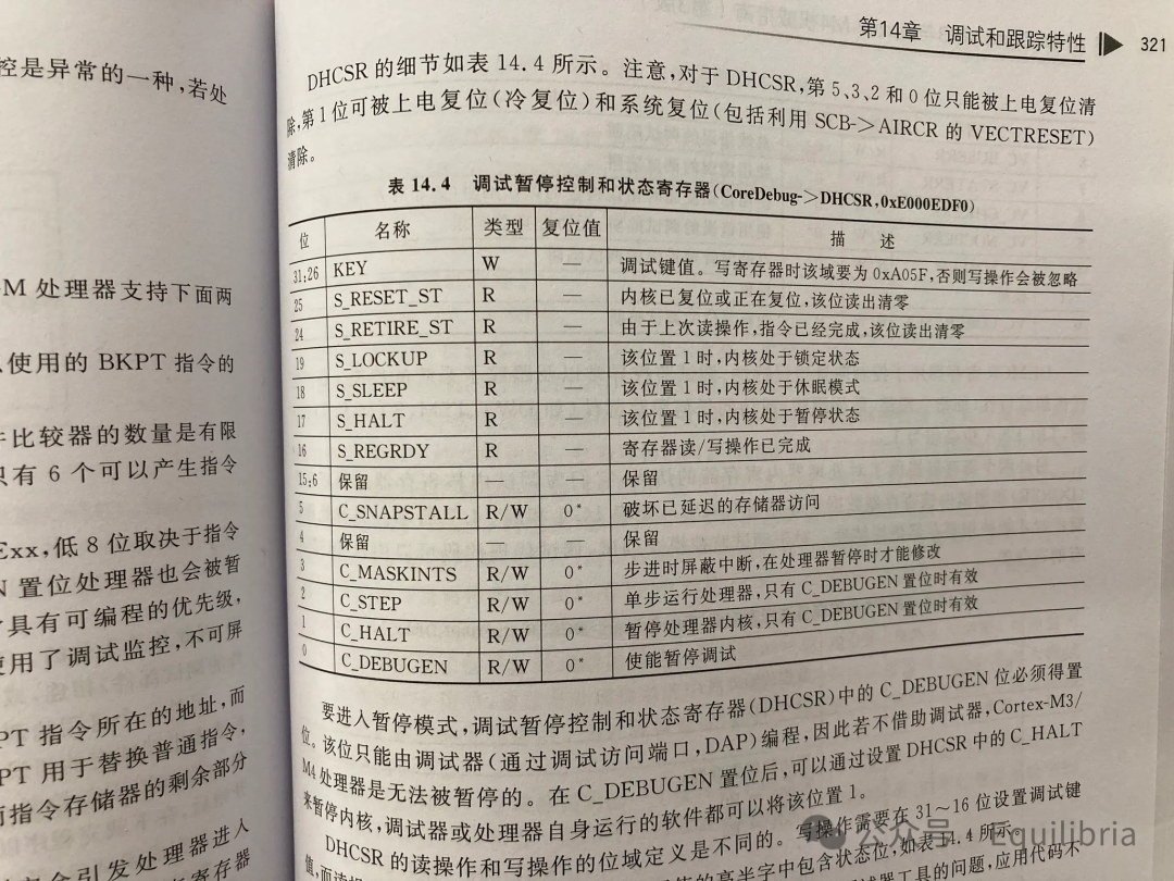
DHCSR register: bit0/2/3/5 can only be reset by POR power-on reset, bit1 can be reset by the core reset.
POR reset will clear the C_DEBUGEN bit, and then Keil will re-initiate the request C_DEBUGEN=1 to maintain the connection.
System reset does not reset SRAM; it only resets the core and other peripherals. __main will reinitialize global variables.
Modify Reset Sequence
-
JLINK
In some cases, it is necessary to customize some operations performed by J-Link.
Script file support allows for custom operations performed by J-Link. Depending on whether the corresponding function exists in the script file, the operations generally implemented will be replaced by the operations defined in the script file.
Place JLinkSettings.JLinkScript in the MDK project directory:
void ResetTarget(void){ Report("J-Link script: ResetTarget"); // Set clock source to hsi MEM_WriteU32(0x50011800, 0x40); // Execute SYSRESETREQ via AIRCR MEM_WriteU32(0xE000ED0C, 0x05FA0004);}Reference:J-Link script files – SEGGER Wiki
-
CMSIS-DAP
In addition to predefined sequences, the PDSC file can include user-defined sequences.
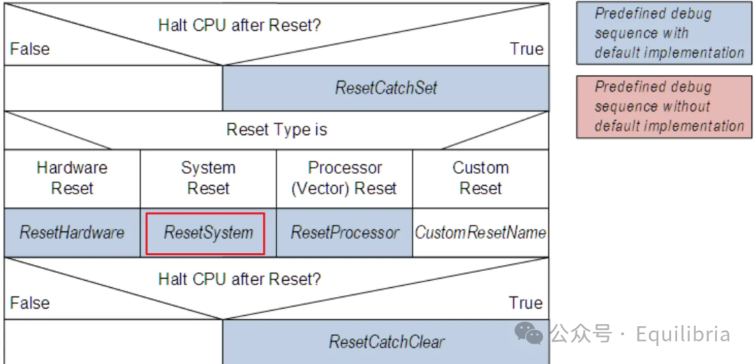
Reference:Debug Description (open-cmsis-pack.github.io)
Add ResetSystem sequence in the PDSC file.
<sequences> <sequence name="ResetSystem"> <block> //Set clock source to hsi MEM_WriteU32(0x50011800, 0x40); //Execute SYSRESETREQ via AIRCR MEM_WriteU32(0xE000ED0C, 0x05FA0004); </block> </sequence></sequences>9. Watchpoint
Watchpoints share hardware comparators with logic analyzers, so to use watchpoints, ensure at least two variable empty slots in the logic analyzer.
A maximum of 4 watchpoints can be set, but the “expression==value” method cannot be used; you can only define a variable and check either read or write, checking both equals using two watchpoints.
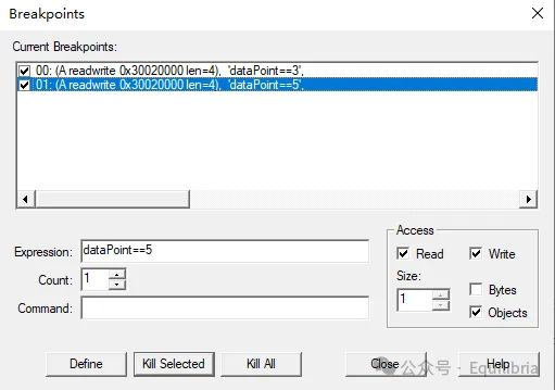
Detailed tutorial on breakpoints and watchpoints:
https://www.keil.com/support/man/docs/uv4/uv4_db_dbg_breakpnts.htm
10. References
1. ARM Cortex-M3/M4 Authority Guide
2. apnt_230_v2.0_STM32F4 Debug Application Manual.pdf
3. an5286_STM32H7x5x7 Dual-Core Microcontroller Debugging.pdf
4. debug_interface_v5_2_architecture_specification_IHI0031F.pdf