Click the blue text above Tansy Laboratory
To get more automotive cybersecurity news
Perface
Recently, I came across some testing materials from the production line and discovered some DFX related content.
While organizing the panorama of the entire security field, debugging security was also mentioned.
For various reasons, I decided to learn about DFX related content, which naturally leads to Coresight.
Today, let’s take a look at Coresight. I’ve recently started to enjoy drawing to organize my thoughts.
Abbreviations
CoreSight SoC-400 is a complete debugging and tracing solution that includes the following components:
-
• Control and access components:
-
• DAP(Debug Access Port): A physical interface for connecting external hardware debugging tools, allowing external debugging tools to access the CPU, CoreSight, DDR, etc. on the chip.
-
• ECT(Embedded Cross Trigger)
-
• Trace data sources: Trace sources are components used in CoreSight to generate trace information. Each trace source component produces a specific format of information that can ultimately be combined and output through trace links to the output port.
-
• PTM(Program Trace Macrocell): Monitors the processor’s operating status and compresses the instruction information executed by the processor for transmission.
-
• STM(System Trace Macrocell): Captures system event information and transmits it in a data trace form to the trace funnel or trace output component.
-
• ETM(Embedded Trace Macrocell): Monitors the processor’s operating status and compresses the instruction information executed by the processor for transmission. Tracks instruction execution, data movement, and PE (Processing Element) events.
-
• Connections:
-
• Synchronous 1:1 ATB bridge:
-
• Replicator: Can multiplex a single input to two branch outputs, allowing the CoreSight system to transmit trace information to two or more outputs simultaneously.
-
• Trace Funnel: Combines information generated by multiple trace sources in the CoreSight system and outputs it as a single stream to the advanced trace busATB. Funnels can be cascaded, and one Funnel can support input from up to 6 trace sources.
-
• Trace output nodes:
-
• ETR(Embedded Trace Router): Stores trace data in the system memory of the debug target platform, with configurable storage space.
-
• ETF(Embedded Trace FIFO): Mainly buffers output data, especially when equivalent data is generated in bursts. The ETF can smooth the output rate of data. The buffer can be configured as FIFO or Circular Buffer; when the FIFO is full, it will backpressure, stopping the source from outputting trace data; when the Circular Buffer is full, it will overwrite.
-
• TPIU(Trace Port Interface Unit): Exports captured data to external debugging adapters, such as DSTREAM.
-
• ETB(Embedded Trace Buffer): A block of RAM within the chip used to store captured trace information. Data stored in the ETB can be accessed through the DAP.
-
• TMC(Trace Memory Controller): Configurable during chip design, can be configured as ETB with the same functionality as the ETB described above. It can also be configured as ETR and ETF.
Timestamp components: Generate timestamps required by CoreSight or the processor. Distributed to multiple destination devices through the Narrow timestamp replicator. Path: Timestamp generator -> Timestamp encoder -> Narrow timestamp replicator -> Timestamp decoder -> CPU/CTI, etc.
-
• Timestamp generator
-
• Timestamp encoder
-
• Timestamp decoder
-
• AMBA AHB trace macrocell (HTM)
-
• Debug access interface (DAP)
-
• Embedded cross trigger (ECT)
-
• AMBA trace bus (ATB)
-
• Bridges and replicators
-
• Trace aggregators (funnel)
-
• Trace port interface unit (TPIU)
-
• Embedded trace buffer (ETB)
-
• Measurement trace macrocell (ITM/STM)
For more detailed information, you can read 【ARM: CoreSight, ETM, PTM, ITM, HTM, ETB and other commonly used term explanations】
1. Coresight
Coresight is a framework proposed by ARM for implementing debugging and tracing for complex SoCs. This architecture includes multiple Coresight components. Numerous Coresight components form a Coresight system.
We can also implement our own Coresight components based on the Coresight architecture.
Each Coresight component must comply with the requirements of the Coresight architecture.
1. A typical Coresight environment
The following is a typical Coresight environment, which includes two ARM cores, one DSP, and numerous Coresight components.
This Coresight component implements debugging and tracing functionality for the core and DSP.
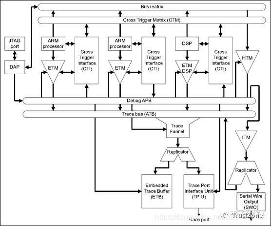
The environment includes a total of 3 paths
-
• Trace path: Outputs internal information from the core and DSP to the outside
-
• Debug path: Implements debugging for the core and DSP
-
• Trigger path: Used for transmitting trigger signals between cores and between core and DSP
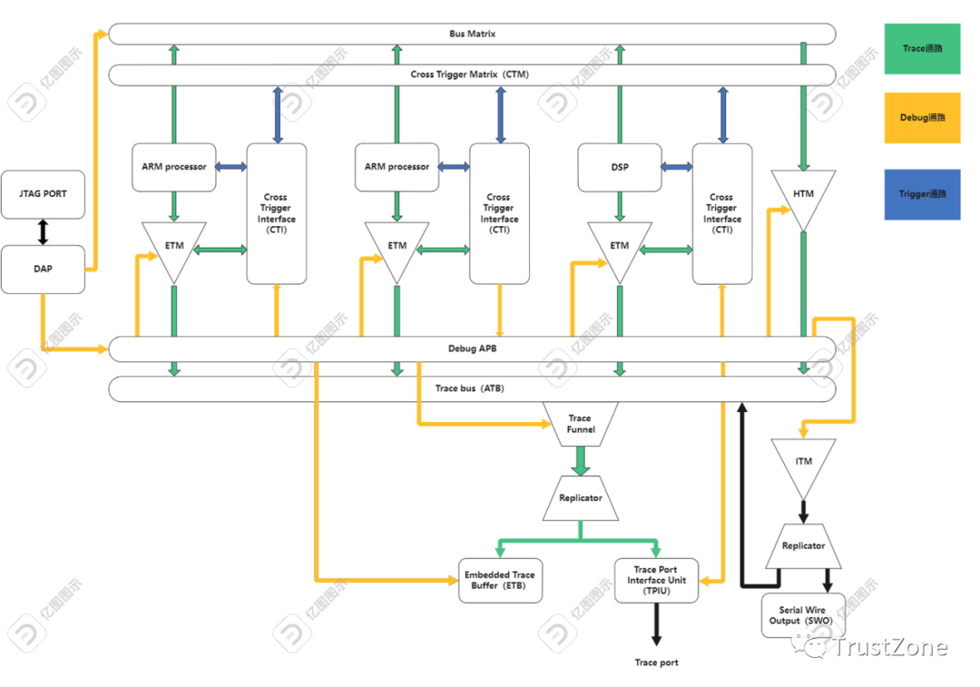
1.1. Trace path
The trace path implements data tracking functionality for the master component, using ETM for tracking.
-
• ETM is responsible for tracking information from the processor and DSP, packaging the information and sending it via the ATB bus to the trace bus.
-
• The trace bus has a trace funnel, which receives data from multiple ATB buses and merges it into a single ATB bus data, sending it to the replicator.
-
• The replicator receives the ATB data and, based on configuration, sends the ATB data to the ETB and TPIU.
1.2. Debug path
The debug path is used for external debuggers to debug the ARM core and DSP.
In the above diagram, only the JTAG port is considered. There is also an SW port.
The DAP receives JTAG data from the external port and converts it into access to the internal AP of the DAP, which then converts it into memory-mapped bus access to access the resources inside the SoC.
In the above diagram, the DAP outputs two memory-mapped buses,
-
• One is the debug APB bus, connected to the debug APB interconnect for accessing the registers of debug components,
-
• One is the system bus, connected to the bus matrix for accessing internal resources of the SoC.
The debug APB interconnect connects to coresight components such as CTI, ETM, HTM, ITM, ETB, TPIU, etc., so external debuggers can access these coresight components through the JTAG port.
The bus matrix generally connects to some peripherals of the SoC, such as memory, serial ports, etc. Therefore, external debuggers can access these peripheral devices through the JTAG port.
1.3. Trigger path
The trigger path is used to send trigger signals to specified components or receive trigger signals from specified components.
This functionality is implemented by CTI and CTM.
CoreSight Cross Trigger Interface (CTI) is a hardware device that brings a single input and output hardware signal, referred to as a trigger, to and from devices, and interconnects them to other devices through a cross-trigger matrix (CTM) to propagate events between devices.Each core and DSP has a CTI component connected, which can send trigger signals to the processor (DSP) and also receive trigger signals from the processor (DSP).
All CTIs are connected to CTM, allowing for mutual sending and receiving of trigger signals between multiple CTIs.
2. Types of Coresight Components
2.1. Control Component
Trigger Coresight components
-
• ECT (embedded cross trigger)
-
• CTI (cross trigger interface): Receives and sends trigger signals
-
• CTM (cross trigger matrix): Passes trigger signals between CTIs
2.2. Trace Sources
Trace Coresight components:
-
• ETM (embedded trace macrocells): Tracks trace information from specified devices (processors, DSPs), with each device (processor, DSP) having its own ETM.
-
• AMBA trace macrocells: Tracks trace information from the AMBA bus.
-
• PTM (program flow trace macrocells):
-
• STM (system trace macrocells): Tracks trace information on the bus interconnect.
2.3. Trace Links
Intermediate Coresight components required for transmitting trace information:
-
• Trace funnel: Merges multiple received ATB bus data into a single ATB bus data.
-
• Replicator: Distributes a single ATB bus data into multiple ATB bus data for transmission.
-
• ATB bridge: ATB bridge, used for data transmission between two different ATB domains.
2.4. Trace Sinks
Coresight components that ultimately receive trace information:
-
• TPIU (trace port interface units): Sends ATB data to the outside through the trace port.
-
• ETB (embedded trace buffers): Buffer for storing ATB data.
-
• TMC (trace memory controller):
Each trace sink can have a trace formatter.
2.5. Debug Access Port
The DAP does not belong to the Coresight components, but we will access Coresight components through the DAP. The DAP includes the following:
-
• APB access port (APB-AP)
-
• AHB access port (AHB-AP)
-
• AXI access port (AXI-AP)
-
• JTAG access port (JTAG-AP)
-
• Serial wire JTAG debug port (SWJ-DP)
-
• JTAG debug port (JTAG-DP)
-
• ROM table
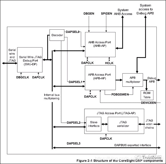
The DAP mainly consists of DP and AP components. DP is responsible for receiving external JTAG or SW data and converting it into access to AP, and access to AP can initiate memory-mapped access. Thus, internal resources can be accessed.
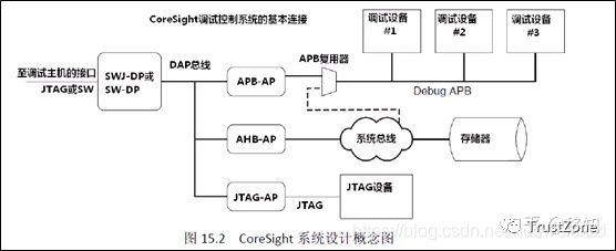
As shown in the figure: The DAP includes three APs
-
• APB-AP: Access to internal debugging devices connected to the debug APB bus.
-
• AHB-AP: Access to devices mounted on the AHB system bus.
-
• JTAG-AP: Access to JTAG devices. This is compatible with older ARM processors, such as ARM9. These older processors used JTAG for debugging. However, current ARM processors no longer use this method and instead use a unified memory-mapped approach for debugging.
In current ARM SoCs, there is generally at least one DAP. A DAP can include 1-256 APs (access ports), which are controlled by the DP.
Only access to AP can be converted into memory-mapped bus to access the internal resources of the SoC.
Memory-mapped bus usually refers to mapping the registers of devices to the memory address space, allowing the CPU to access and control these devices by reading and writing these memory addresses. This method simplifies the access and control of devices, allowing the CPU to access these devices as if accessing memory.
There is a SELECT register in the DP, which is used to select which AP the DP accesses.
In the DAP, there can be multiple APs, but only one AP can be accessed at a time. This is because the APs need to be numbered, and the value is in the APSEL bit field. Since this bit field has 8 bits, a DAP can have a maximum of 256 APs.
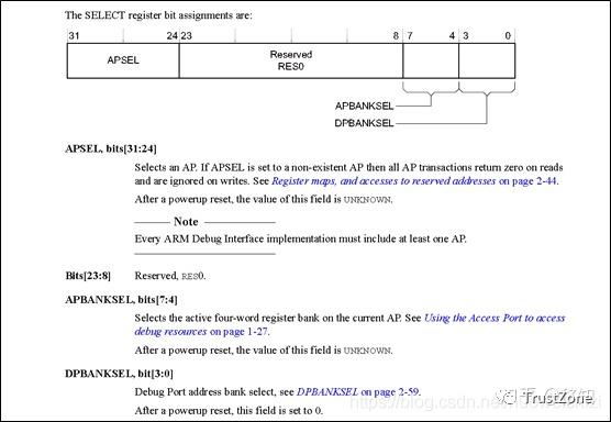
The internal structure of the DAP is shown in the figure above:
It includes a DP and three APs, namely AHB-AP, APB-AP, and JTAG-AP.
The DP connects to external debuggers through JTAG or SW pins and communicates with external debuggers.
The DP receives JTAG or SW data sent by external debuggers, converts it into access to internal APs. After passing through the decoder module, it determines which AP to access and sends the access information to the corresponding AP.
After the AP receives the DP’s access, it converts it into the corresponding bus access to access internal resources.
Then the access information is returned to the DP, which sends the access information back to the external debugger through JTAG or SW.
The above is the entire content of this article. I hope that after reading it, you can have a macro understanding of Coresight.