
Currently, there is a growing desire among humans to retire the “Von Neumann architecture”. Due to the issues of memory wall and power wall, the Von Neumann architecture is increasingly hitting a bottleneck.
Neuromorphic chips are one of the routes to break through the “Von Neumann architecture”. They are chips that highly simulate the computational principles of the human brain. If neuromorphic chips are made to resemble the human brain more closely, they will be given a new name—Neuromorphic Computing, which is an important development path for digital chips and AI computation.
Neuromorphic computing is seen as a disruptive force in the edge AI industry because its power consumption is incredibly low. A perfect neuromorphic chip could solve problems with energy consumption that is 1000 times lower than traditional solutions, meaning we can pack more chips to solve larger-scale problems within a fixed power budget.
Of course, current neuromorphic computing has not yet reached such levels, but it does have the capability to reduce power consumption by several times or even dozens of times compared to existing chips. For example, IBM previously launched the neuromorphic chip “NorthPole”, which achieved five times the energy efficiency compared to the Nvidia H100 GPU implemented on a 4nm node.
Now, neuromorphic computing is also beginning to penetrate the edge AI field, even changing MCUs.
Innatera Launches First Commercial Neuromorphic MCU
Recently, the startup Innatera announced the launch of a new type of spiking neural processor (SNP). Pulsar is a neuromorphic signal processor designed to perform edge AI inference with high energy efficiency, achieving a latency reduction of 100 times compared to traditional AI processors.
Additionally, from a power consumption perspective, the system uses an internal low-power PLL and software-controlled voltage domains to reduce dynamic and standby power consumption. Multiple sleep modes further optimize energy consumption during idle periods.
Innatera claims that the power consumption of this processor is 500 times lower than that of traditional AI processors.
The underlying architecture of Pulsar integrates a fully programmable spiking neural network (SNN) structure optimized for asynchronous, sparse data computation. To this end, Pulsar provides a heterogeneous computing architecture that separates SNN, CNN, and traditional CPU tasks to optimize workload partitioning.
Innatera designed the processor to be flexible, supporting neuron and synapse-level parameterization across different network topologies to specifically meet the needs of spatiotemporal workloads such as audio and vibration sensing. To support mixed workloads, SNN structures run alongside a floating-point 32-bit RISC-V CPU and a 32-MAC CNN accelerator. The FFT/IFFT engine provides additional computational power for time-frequency domain applications.
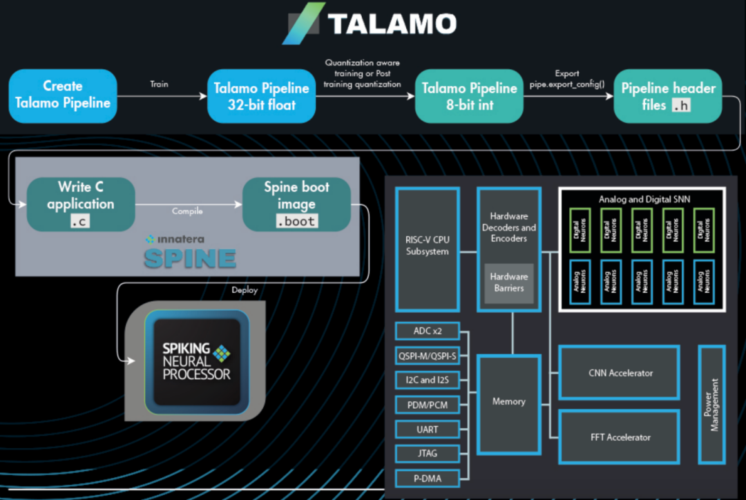
The memory subsystem of this processor includes 384 KB of general-purpose SRAM, 128 KB dedicated to CNN computation and 32 KB reserved SRAM to maintain application state through low-power transitions. Integrated peripheral support includes I2C, UART, SPI, JTAG, ADC, camera interfaces, and GPIO, supported by a distributed DMA engine to facilitate peak data processing. The supply voltage is 1.6V, the system frequency is 160MHz, and the package size is 2.8mm x 2.6mm/36pin WLCSP, with an operating temperature of -40℃~125℃.
On the software side, Pulsar is supported by the Talamo SDK, which integrates model training based on PyTorch with direct hardware mapping. Developers can deploy models using the native Python compiler or the standard GCC toolchain for RISC-V.
Polyn’s First Neuromorphic Analog Signal Processing Chip Tape-Out
Recently, Polyn Technology announced the successful tape-out of its first chip based on a proprietary neuromorphic analog signal processing platform (Neuromorphic Analog Signal Processing, NASP), while the NASP chip has entered the certification stage and is expected to be officially launched in the second quarter of 2025.
This chip achieves ultra-low power consumption and real-time signal processing capabilities, with power consumption below 100μW during signal inference, and in certain application scenarios such as the NeuroVoice VAD model, it can even drop to 30μW.
Such low power consumption makes it very suitable for applications in power-constrained environments such as headphones, wearable devices, smart tires, and predictive maintenance sensor nodes. Additionally, NASP can reduce the amount of raw data by up to 1000 times, significantly enhancing privacy protection and reducing reliance on cloud services, especially suitable for fields with high data security requirements such as healthcare. In the technical documentation, NASP released results comparing the inference of MobileNet V.2 against Raspberry Pi 3B+ and JETSON TX1.

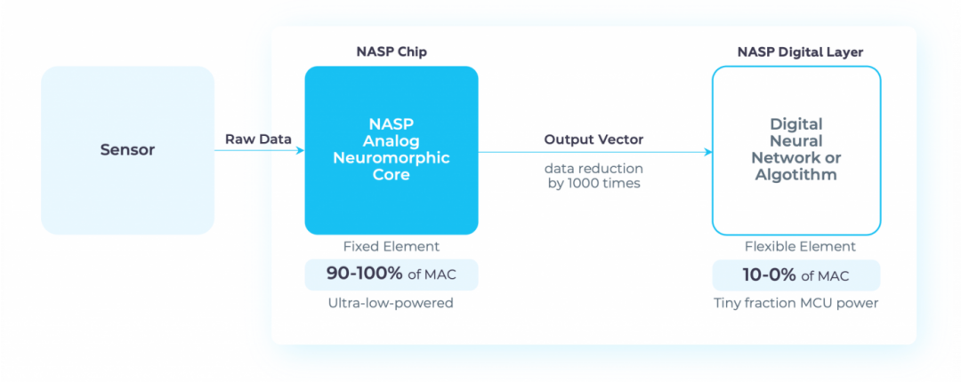
NASP is the core of Polyn’s technological innovation. It is a hybrid analog-digital architecture that mimics the distributed, ultra-parallel operation of biological neurons through analog circuits. The system consists of operational amplifiers and programmable resistors, capable of performing native inference on sensor data directly without relying on a central processor or digital pre-processing of signals.
Unlike traditional sensor data processing methods, NASP can filter and compress at the raw audio input stage, outputting only the key feature vectors for subsequent processing. This approach not only enhances efficiency but also achieves a “understanding” of the signals, significantly reducing bandwidth requirements and cloud dependency.
When acting as an edge signal sensor, it can process raw sensor data using neuromorphic computing without any digitization of the analog signals. For this reason, the company refers to it as the first neuromorphic analog TinyML chip that can be used directly next to the sensor without an analog-to-digital converter (ADC).
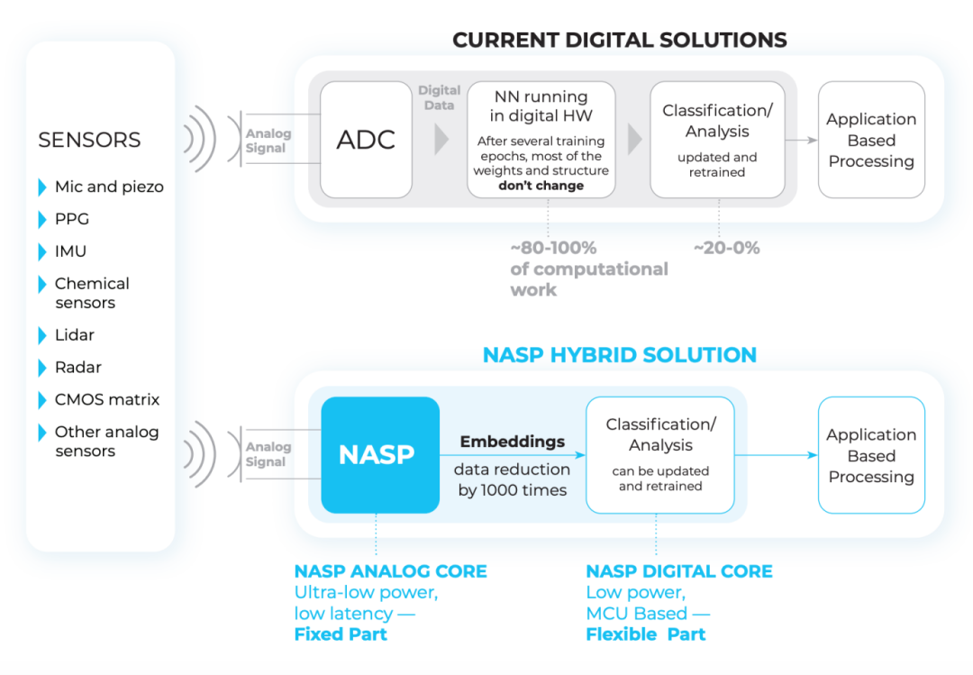
NASP platform adopts a “fixed + flexible” dual-module structure:
-
Fixed part: implemented through hardwired analog circuits, responsible for extracting key features from raw sensor data;
-
Flexible part: implemented using standard digital logic or low-power microcontrollers, responsible for classification and interpretation.
This hybrid architecture introduces transfer learning at the hardware level. Developers only need to retrain the flexible part to quickly adapt to new tasks, such as using accelerometer data originally intended for gait recognition for fall detection, significantly shortening product iteration cycles and reducing overall complexity.
Polyn has independently developed a compiler toolchain for NASP, and in the design process, Polyn utilizes Cadence’s Virtuoso and Innovus tools to integrate analog and digital circuit design, achieving tape-out on a 55-nanometer CMOS process.
Currently, Polyn is deeply collaborating with industry-leading companies such as SkyWater, Bridgestone, Infineon, and TDK. Although its first chip focuses on voice processing, potential future application scenarios include vibration analysis, biological signal interpretation, and human-computer interaction.
In December 2023, Infineon disclosed its collaboration with Polyn, with both parties working together to develop advanced tire monitoring products, where Infineon will provide a new generation of TPMS sensors with tire vibration signal detection capabilities, utilizing Polyn‘s NFE to preprocess the sensor’s vibration data.

Fraunhofer Develops Edge AI Accelerator
In March of this year, the Fraunhofer Institute for Integrated Circuits IIS developed an AI chip for processing spiking neural networks (SNN). The inference accelerator of the spiking neural network SENNA is inspired by brain functions and consists of artificial neurons that can directly process electrical pulses (spikes). Its speed, energy efficiency, and compact design make it possible to use SNN directly in the place where data is generated (i.e., edge devices).
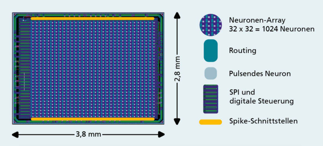
SENNA is a neuromorphic chip designed for quickly processing low-dimensional time series data in AI applications. Its current version consists of 1024 artificial neurons and has a chip area of less than 11 mm². The chip’s response time is as short as 20 nanoseconds, ensuring precise timing, especially in edge time-critical applications.
Thus, its advantages are truly evident in real-time evaluation of event-based sensor data and closed-loop control systems; for example, when using AI to control small motors.SENNA can also be used to achieve AI optimized data transmission in communication systems. There, AI processors can analyze signal flows and adjust transmission and reception programs as needed to improve transmission efficiency and performance.
One reason for the energy efficiency of SNN is that neurons are only activated by a small number of events. Through its spiking neurons, SENNA fully utilizes this energy-saving advantage. Due to its fully parallel processing architecture, artificial neurons can accurately map the temporal behavior of SNN. SENNA can also directly process spike-based input and output signals through its integrated spike interface. In this way, it can seamlessly adapt to event-based data streams. “With its novel architecture, SENNA addresses the trade-offs between energy efficiency, processing speed, and versatility that other edge AI processors cannot match. This makes it particularly suitable for resource-constrained applications that require extremely fast response times in the nanosecond range,” explained Michael Rothe, manager of the Fraunhofer IIS Embedded AI Group.
The current SENNA reference design is designed for a 22nm manufacturing process. This means that SNN processors can be used as chips in various applications and can be implemented economically and efficiently. Its design is scalable and can adapt to specific applications, performance requirements, and special features of target hardware before chip production. But even after chip manufacturing is completed, SENNA retains maximum flexibility, as it is fully programmable. The SNN models used can be changed and re-uploaded to SENNA repeatedly. To make it as easy as possible for developers to implement their AI models, Fraunhofer IIS also provides a comprehensive software development toolkit for SENNA.
What is Neuromorphic Computing?
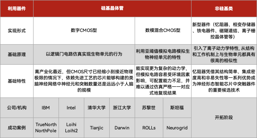
Currently, the structures of neuromorphic chips around the world are basically consistent, consisting of three parts: neuron computation, synaptic weight storage, and routing communication. However, the key points lie in the highlights—one is the model, and the other is the device.
First, in terms of the model, current neuromorphic chips generally adopt SNN (spiking neural networks). Compared to traditional neural networks, spiking neural networks (SNN) have a more “neural” characteristic structure. Traditional neural networks rely on matrix convolution or matrix multiplication to achieve signal propagation, while SNN adopts a synaptic structure closer to the human brain during propagation. In SNN networks, when the pulse signal accumulates to a certain level, the neuron sends a signal representing “1” to the next neuron, after which its membrane potential returns to a lower level and enters a refractory period during which it cannot send signals again.
For SNN, spatiotemporal dynamics is an important characteristic. By introducing the time dimension, SNN can achieve asynchronous computation. SNN excels at processing spatiotemporal dynamic information, especially suitable for integration with event-driven sensors (such as dynamic vision sensors DVS). Currently, most manufacturers choose a heterogeneous solution of SNN+CNN to cope with different scenarios.

Secondly, in terms of device implementation, based on materials, devices, and circuits, there are three factions: neuromorphic systems dominated by analog circuits (mixed-signal CMOS), fully digital circuit neural systems (digital CMOS), and mixed-signal neuromorphic systems based on new devices (memristors are candidate technologies).
Digital CMOS is currently the most industrially viable form; on one hand, the technology and manufacturing maturity are high, and on the other hand, there are no concerns and limitations associated with analog circuits. However, digital CMOS is still only the initial stage of neuromorphic chips and does not yet fully simulate the neural devices of the human brain.
Mixed-signal CMOS is Polyn’s implementation method. In comparison, this approach can directly omit the ADC and process the raw data from sensors directly through programmable resistors.
Memristors are a technology currently being researched in the scientific community. The allure of memristors lies in the fact that they are not only storage units but can also perform computations! Imagine if your hard drive could not only store data but also perform deep learning computations directly, then the speed of AI training would be greatly enhanced. This characteristic of memristors makes them a core component of compute-in-memory architectures. Memristor compute-in-memory architectures are rapidly developing and are expected to enter commercial applications in the next 5~10 years.
Types of neuromorphic chips and their R&D progress, table compiled by Electronic Engineering World
Currently, many domestic companies are also researching neuromorphic computing chips, with their main goal being edge AI.
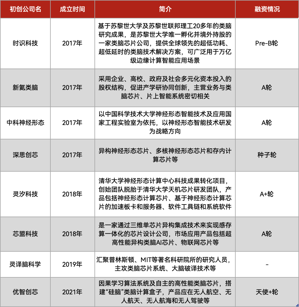
Domestic research includes top universities and institutions such as Tsinghua University, Zhejiang University, Fudan University, and the Chinese Academy of Sciences, while in the past two years, numerous startups have emerged, such as Lingxi Technology, Shishi Technology, and Zhongke Neuromorphic. Among them, Tsinghua University’s Tianji chip and Zhejiang University’s Darwin chip are the most representative.
Edge AI is Being Disrupted
In summary, brain-inspired neuromorphic computing is disrupting edge AI scenarios.
Unlike the traditional Von Neumann architecture, neuromorphic chips simulate the neurons and synaptic structures of the human brain, featuring ultra-low power consumption and parallel processing capabilities, making them particularly suitable for AI applications on edge devices.
After all, a hundredfold improvement in energy efficiency is too appealing; who wouldn’t want that?
Currently, neuromorphic chips from Intel’s Loihi, IBM’s TrueNorth, and others have demonstrated tremendous potential in edge AI scenarios.
Moreover, the manufacturers mentioned above have already begun to formally attempt to use neuromorphic chips in commercial scenarios. Although due to cost, development difficulty, and other considerations, they may not completely replace existing MCUs or embedded chips, they will certainly find strong applications in specific scenarios. A new revolution in edge is about to arrive.
· END ·
Follow the subscription account of EEWorld: "Robot Development Circle"
Reply "DS" to receive the complete version of "DeepSeek: From Beginner to Expert"

Scan to add the assistant and reply “robot”
Join the group to exchange experiences face-to-face with electronic engineers