Click the blue text to follow us

1. Development of the 80C51 Microcontroller
MCS-51 is the name of the microcontroller series, which includes various chip models; the 80C51 is both the series name and a specific chip model.
The early 80C51 series chip models corresponded exactly to MCS-51. They both have two sub-series, namely the basic 51 sub-series and the enhanced 52 sub-series.
The 80C51 is an improvement over MCS-51, specifically in the semiconductor integrated circuit technology used. MCS-51 uses HMOS technology, which is a high-density short-channel MOS semiconductor integrated technology, while the 80C51 uses CHMOS technology, which is a complementary metal-oxide HMOS semiconductor integrated technology. The improvement in integrated technology gives the 80C51 significant advantages such as strong anti-interference ability and low power consumption.
(1) Functionally Simplified Chips
(2) Functionally Enhanced Chips
2. Enhancements of 8-bit Microcontroller Functions from 8×C552
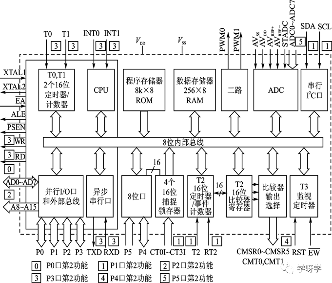
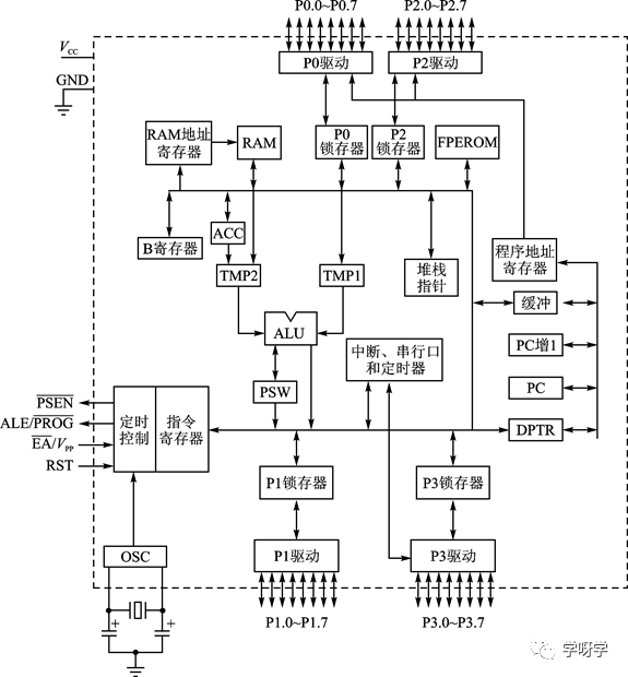
The hardware structure of the 8×C552 chip is built on the 80C51 core with additional functional components. Here, the 83C552 chip is used as an example, and the hardware structure block diagram is shown below.
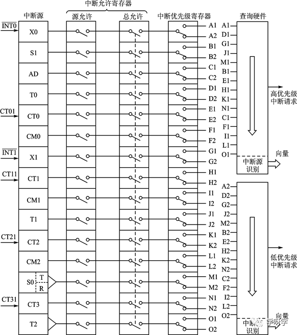
Due to the increase in interrupt sources, both the interrupt enable register and the interrupt priority control register have increased to two. For the interrupt enable register, the original from the 80C51 is renamed IE0, and the newly added one is called IE1. For the interrupt priority control register, the original from the 80C51 is renamed IP0, and the new one is called IP1.
The hardware query order is: External Interrupt 0 (X0) → Timer 0 Interrupt (T0) → External Interrupt 1 (X1) → Timer 1 Interrupt (T1) → Serial Interrupt (S0) → I2C Interrupt (S1) → Capture 0 Interrupt (CT0) → Capture 1 Interrupt (CT1) → Capture 2 Interrupt (CT2) → Capture 3 Interrupt (CT3) → A/D Interrupt (AD) → Compare 0 Interrupt (CM0) → Compare 1 Interrupt (CM1) → Compare 2 Interrupt (CM2) → Timer 2 Interrupt (T2).
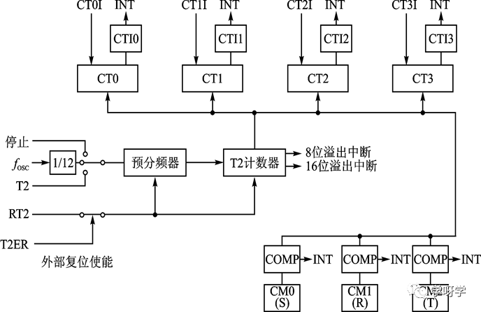
8×C552 Event Capture and Event Timer Output Logic Structure
For microcontroller application systems, reliability is crucial. This is because the field environment for microcontroller applications is often harsh, making it prone to failures due to interference; once a failure occurs, it can lead to system loss of control and even extremely serious consequences.
To improve system reliability, in addition to taking sufficient hardware measures, the execution of the program should also be monitored, as the reliability of the system ultimately reflects the execution of the program. The most common program execution faults are “runaway” and infinite loops. For these program execution faults, it is necessary to detect them in a timely manner and also be able to recover automatically to achieve system self-rescue. Common methods include inserting trap programs and setting up a “watchdog”.
The watchdog timer of the 8×C552 consists of an 8-bit timer T3 and an 11-bit prescaler, where the prescaler is the low part of the counting structure and the timer is the high part. The counting pulse of the watchdog timer comes from the internal clock of the chip, incrementing by one during each machine cycle.
When the watchdog timer overflows, it can generate an effective reset signal, thus resetting the microcontroller system, which is the function of the watchdog timer.
The program should assign a value to the watchdog timer within a time interval shorter than the monitoring cycle to prevent overflow. When a fault occurs and the program cannot run normally, the watchdog timer will overflow due to the inability to assign values on time, resetting the system.
The 8×C552 has two pulse-width modulation outputs, composed of a prescaler (PWMP), an 8-bit up counter, two pulse width registers (PWM1, PWM0), two comparators, and related logic circuits. Its structural block diagram is shown below.
The output pulse width interval (duty cycle) of the PWM is programmable, with data written into PWM1 and PWM0 through the program. The repetition frequency is determined by the prescaler PWMP.
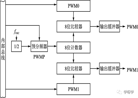
The period (or frequency) of the PWM output pulse is controlled by the prescaler PWMP. The PWM counter increments by one for each state cycle, with a maximum count value of 255 for the 8-bit counter. Therefore, the frequency fPWM of the PWM output pulse can be calculated using the following formula:
fPWM= fosc/2×(PWMP+1)×255
Using this formula, as long as the clock frequency and the prescaler value are known, the PWM pulse period can be calculated in microseconds.
The width of the PWM square wave pulse is determined by the pulse width registers (PWM1 and PWM0). Since PWM generates square waves through counting and comparison, changing the contents of the pulse width registers will change the pulse width.
The percentage of the pulse width in the entire pulse period is called the duty cycle. Since the width of the PWM pulse is controllable, its duty cycle is also adjustable.
The most basic application of PWM is generating square waves, and the vast majority of PWM applications are based on filtering the PWM square wave. For example, by simple processing of the PWM wave, a continuously varying analog signal can be obtained, achieving D/A conversion functionality, as shown in the circuit below.
3. Flash Memory and Its Applications in Microcontrollers
Flash memory, fully known as flash programmable/erasable read-only memory, is abbreviated as flash memory or FlashROM, and can also be referred to as FPEROM (Flash Programmable and Erasable Read Only Memory). It was successfully developed by Intel in the late 1980s.
Flash memory is writable and non-volatile, so it is commonly used as read-only memory.
In addition to having high density, low power consumption, non-volatility, high reliability, long retention time, and strong encryption capabilities, its advantages are more evident in online programming functionality.
Flash ROM and E2PROM both use electrical signals for programming and erasing, and can be repeated.
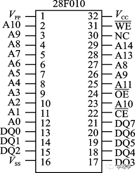
Flash memory chips can have storage capacities ranging from 2 to 16 KB, with recent chips appearing that have capacities from 16 to 64 MB. Here, a typical flash memory chip, the 28F010, is introduced. The storage capacity of the 28F010 flash memory chip is 128 KB, and the pin arrangement is shown in the diagram below.
-
A16~A0: Address pins. During the write cycle, their contents are latched by the internal address latch.
-
DQ7~DQ0: Data pins. When the chip is not selected, the pins are in a high-impedance state.
-
/CE: Chip select signal, active low. When CE=0, the chip is selected, activating the control logic and related circuits inside the chip. When CE=1, the chip is not selected, reducing power consumption to standby mode.
-
/OE: Output enable control signal, active low. During the read cycle, when OE=0, the output buffer is enabled, and the read data is output through the buffer.
-
/WE: Write signal, active low. Used to control write operations to the command register and storage array; the address is latched on the falling edge of WE pulse; the data is latched on the rising edge.
-
VPP: Erase/program voltage.
-
VCC: Main power supply, +5 V.
-
VSS: Ground.
-
NC: No connect pin.
The core of the 28F010 is a 1,048,576-bit storage array, along with corresponding decoding and gating circuits. Other parts are auxiliary circuits for online erasing and programming. The internal hardware structure of the 28F010 is shown in the diagram below.
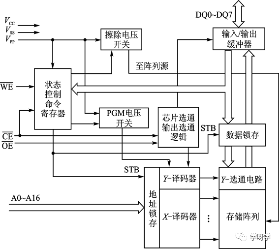
The structure of the 28F010 chip
Online erasing and programming are mainly achieved through the programming pin VPP and the command register. When VPP is not supplied with programming voltage (usually grounded), the command register content is set to the default value (i.e., data read command), and the storage chip is in read-only mode. At this point, only read operations can be performed on the flash memory, and write operations cannot be performed. To perform online erasing and programming operations, the VPP pin must be connected to a high programming voltage (+12 V). At this time, in addition to normal data read operations on the flash memory, erasing and programming operations can also be performed, including erasing and programming the storage array and reading programming verification data. However, each operation requires writing the corresponding command to the command register.
Flash microcontroller chips refer to microcontroller chips with flash memory as the internal program storage. A typical flash microcontroller chip in the 80C51 series is the 89C51.

The structure of the 28F010 chip
-
Contains 4 KB of flash memory.
-
128 B of internal RAM units.
-
Two 16-bit timers/counters.
-
The interrupt system still has 5 interrupt sources with a two-level priority structure.
-
4 8-bit I/O ports, i.e., 32 programmable port lines.
-
Programmable full-duplex serial port.
-
Wide range of operating voltage, with VCC allowing a variation range of 2.7 to 6.0 V.
-
Can be set to standby and power-down states.
-
Oscillator and clock circuit with full static operation mode, clock frequency can be 0 Hz to 24 MHz. Full static operation mode indicates that it does not require continuous clock timing; during waiting for internal events, the clock frequency can be reduced to 0.
(3) Simplified Chip of AT89C51

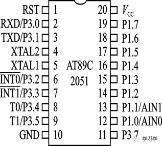
The AT89C2051 does not have parallel expansion capabilities, so only P1 and P3 remain as I/O ports. However, the AT89C2051 chip includes an analog comparator, with the comparator using pins P1.1/AIN1 and P1.0/AIN0 as the positive and negative inputs for the analog signal. Since P3.6 is used as the comparator output, the chip no longer has the P3.6 pin. The diagram is shown below.
The flash memory in the microcontroller chip is in an erased state by default, with all address units containing FFH. There are two programming methods: one is using a dedicated programming device, and the other is utilizing the system’s own resources.
Using the chip’s own resources for programming is also known as In-System Writing (ISW), or online programming.
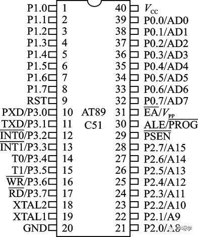
To achieve flash memory programming, the relevant address, data, and control signals must be prepared in advance. The programming interface signals of the AT89C51 chip FPEROM are shown in the diagram below.
-
P0.7~P0.0: Code input during programming, code output during verification.
-
P1.7~P1.0 and P2.3~P2.0: Address for storage array unit, since the flash capacity of the AT89C51 is 4 KB, 12 bits of address are required.
-
P3.7, P3.6, P2.7, P2.6: High and low level combination settings.
-
ALE/PROG: PROG is the programming pulse signal.
-
EA/VPP: VPP is the programming power supply.
For the AT89C51 chip, there are two programming voltages: one is +5 V, which can connect VPP directly to the chip’s VCC; the other is +12 V, where VPP is connected to a separate +12 V power supply. The +5 V programming voltage makes online programming of user systems possible, providing convenience for users; while the +12 V programming voltage is used for dedicated programming devices.
Taking the online programming of the flash memory in the AT89C51 user system as an example, the programming process includes the following main steps:
- Connect VPP to the +5 V power supply.
- Write the address of the programming unit.
- Write the data of the programming unit.
- Provide the necessary programming signals and level combinations.
- Issue the programming pulse.

Long press the image to follow
Discover more exciting content
WeChat ID: Mechanical-knowledge