The TFT-LCD technology is based on semiconductor IC manufacturing processes. The uniqueness of TFT-LCD technology lies in its use of glass substrates instead of traditional silicon wafers. For the TFT manufacturing process, thin film formation, such as CVD, PVD, etc., are very important steps. During the assembly process of color filters and TFT substrates, the ODF process has been developed and applied to large-size LCDs.
In the following sections, we will introduce the process of TFT, Cell, and Module step by step.
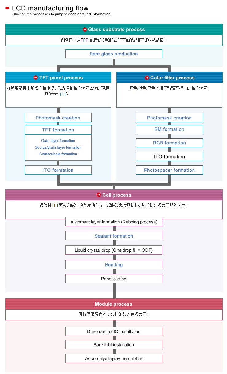
1. TFT panel process
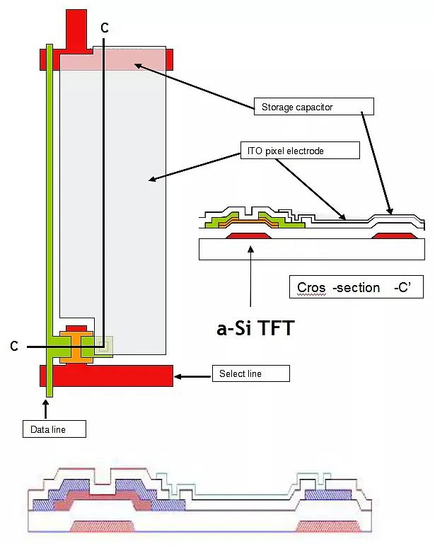
Conventional liquid crystal screens use back-channel etched (BCE) TFT structures for display pixels. The specific structure is shown in the figure below:
The main process flow of the back-channel etched TFT structure array panel can be divided into 5 steps (5 exposures) according to the sequence of the layers to be made and the interrelationship between the various layers.
The first layer is the Gate electrode.
The second layer is the Gate insulating layer
The third layer is the Source/Drain electrodes
The fourth layer is the Contact Hole
The fifth layer is the ITO electrode
The process types are as follows:
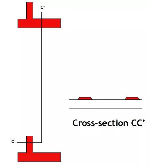
The first step: Formation of Gate and scanning lines
This includes: Gate layer metal sputtering, Gate photolithography, Gate wet etching, and other processes. After these processes, scanning lines and gate electrodes, i.e., Gate electrodes, are formed on the glass substrate. The resulting pattern after the process is shown in the figure below:
The photolithography technology copies the mask pattern structure onto the glass substrate to be etched. The three main processes are: photoresist coating, exposure, and development.
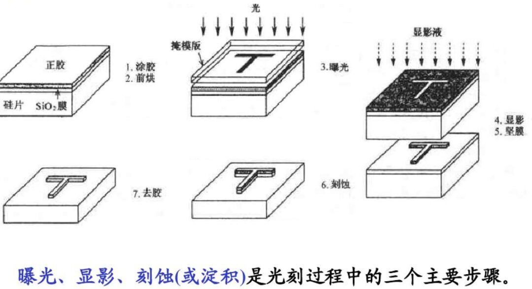
Wet etching: Wet etching uses appropriate corrosive solutions to remove the film layers that need to be removed through chemical reactions.

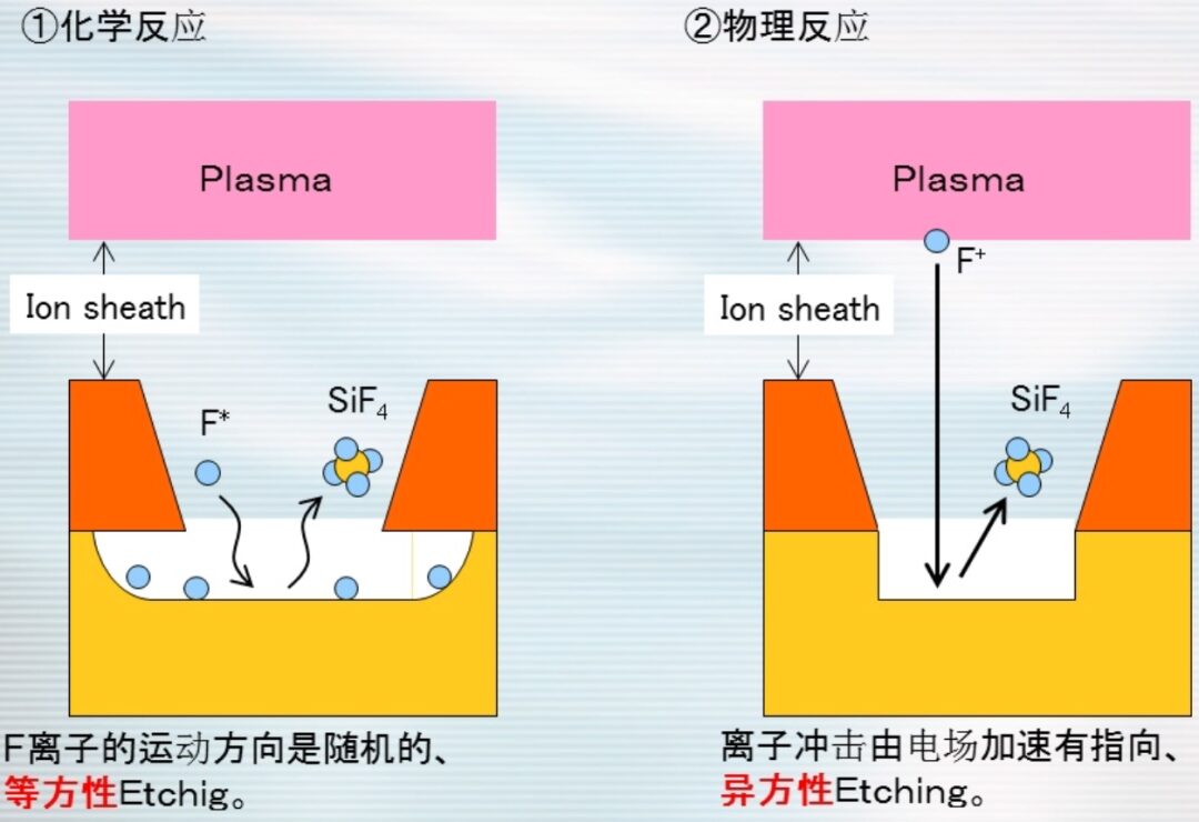
Dry etching: This uses process gases and chemical reactions with thin films, as well as plasma bombardment of the thin films to achieve the purpose of removing the film layers.
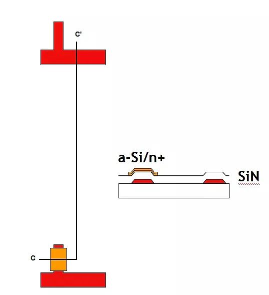
The second step: Formation of Gate insulating layer and amorphous silicon islands
This includes: PECVD three-layer continuous film formation, island photolithography, island dry etching, and other processes. After these processes, amorphous silicon islands for TFT are formed on the glass substrate. The resulting pattern after the process is shown in the figure below:
PVD (Physical Vapor Deposition) is an advanced surface treatment technology widely used internationally. Its working principle is to utilize gas discharge under vacuum conditions to partially ionize gases or evaporated substances. At the same time, with the bombardment of gas ions or ions of evaporated substances, the evaporated substances or their reaction products are deposited on the substrate. Currently, the most commonly used PVD technologies mainly include magnetron sputtering, multi-arc ion plating, and evaporation.
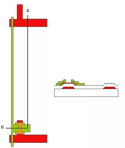
The third step: Formation of Source/Drain electrodes, data electrodes, and channel
This includes: S/D metal layer sputtering, S/D photolithography, S/D wet etching, channel dry etching, and other processes. After these processes, the source, drain electrodes, channels, and data lines of the TFT are formed on the glass substrate. At this point, the TFT has been completed. The resulting pattern after the process is shown in the figure below:
The fourth step: Formation of passivation insulating layer and vias
This includes: PECVD film formation, photolithography, via dry etching, and other processes. After these processes, the TFT channel protection insulating layer and conductive vias are formed on the glass substrate. The resulting pattern after the process is shown in the figure below:
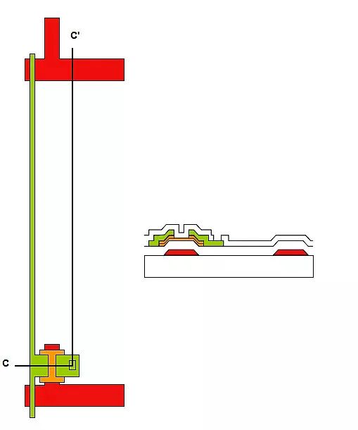
The fifth step: Formation of transparent pixel electrodes (ITO)
This includes: ITO transparent electrode layer sputtering, ITO photolithography, ITO wet etching, and other processes. After these processes, transparent pixel electrodes are formed on the glass substrate. The resulting pattern after the process is shown in the figure below:
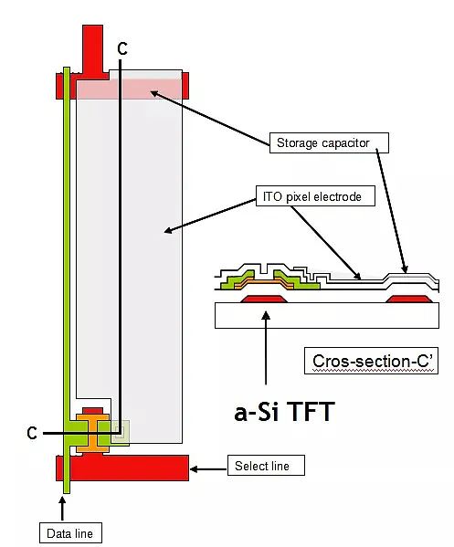
At this point, the entire array process is completed. In simple terms, the array process of 5 exposures consists of: 5 film formations + 5 etchings.
2. CF process
Color filters can be produced by various methods; photolithography is a typical method. In photolithography, the color filter is produced by exposing a glass substrate coated with photosensitive color resist through a photomask. The resist is hardened to form the RGB pattern of the LCD.
1. Formation of black matrix (low-reflective chromium or resin)

First, a black matrix is formed to prevent any leakage of backlight and RGB color mixtures.
2. Color resist coating
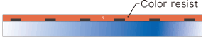
The color resist is coated over the entire surface of the glass substrate.
3. Exposure
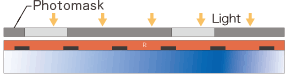
To make the pattern insoluble, it is cured with ultraviolet light through a photomask.
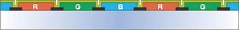
4. Development and baking

After removing unnecessary parts of the color resist with a developer solution, the pattern is cured by baking.
★ Repeat steps 2 to 4 three times (for RGB).

5. Formation of ITO layer
The ITO layer (transparent conductive layer) is formed by the sputtering method.
6. Formation of photo spacer (PS)
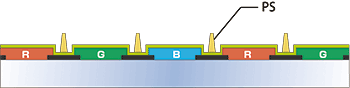
PS is formed to more thoroughly control the cell gap between the two glasses (color filter and TFT array) for improved image quality.
Functions:
1. Appropriate mechanical strength
2. High contrast
3. Reduces scratches on color filters caused by spherical spacers due to vibration
4. Good uniformity
3. Cell process
The Cell in the middle section uses the previous Array glass as the substrate, combined with the colored filter glass substrate, and fills liquid crystal (LC) between the two glass substrates.
1. PI Coating
Provides the alignment and pre-tilt angle substrate required for liquid crystal molecules in the Cell.
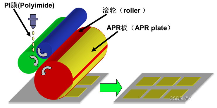
2. Rubbing
Using an aligning cloth to rub the PI film over the glass substrate, grooves are created to align the liquid crystals in a specified direction between the upper and lower aligning films.
Like the PI process, rubbing especially requires the elimination of ESD.
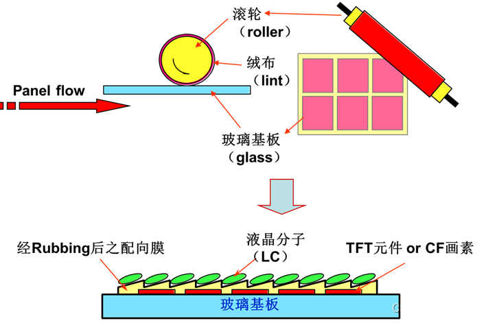
The pre-tilt angle (Pre-tilt Angle or TBA: Tilt Bias Angle) characteristic indicates that the arrangement of liquid crystal molecules on the aligning film is not parallel to the film surface, but that one end of the molecules is tilted relative to the film surface in the rubbing direction, and the angle is called the pre-tilt angle. Without the pre-tilt angle, under an external electric field, the liquid crystal molecules can stand up randomly from two directions, which will cause poor display.
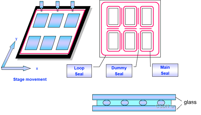
3. Frame adhesive
Components of frame adhesive:
(1) Main component: sealant
(2) Silicon balls: have a certain height and act as spacers
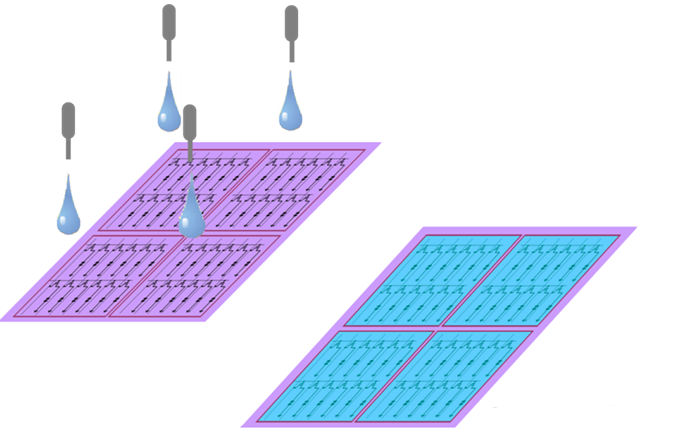
4. Liquid crystal injection
The method of liquid crystal filling is one-drop-fill.
5. Thermal pressing
The array glass is pressed and bonded with the color resist glass.
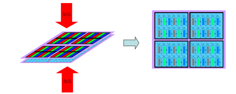
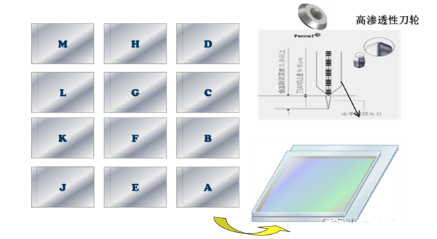
6. Cutting and splitting
In the production of liquid crystal panels, it is not possible to produce one by one, as this would be too inefficient. Therefore, multiple pieces are processed at once and separated by cutting.
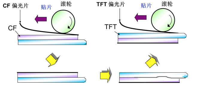
7. Attachment of polarizers
After that, the bonding IC and FPC are assembled, along with the backlight module and the machine casing, which are relatively simpler processes compared to the high-precision processes before.
4. Module process
The main process of the module includes: COG, FPC bonding, assembly, etc. The following will introduce each one.
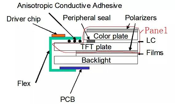
1. COG and FPC bonding
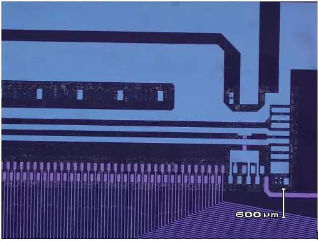
COG (Chip on Glass) and FPC (Flexible Printed Circuit) are a way of connecting circuits. Due to the large number of electrodes, one-to-one wiring connections are very difficult. The usual method is to make the leads on the glass into an array, and the leads on the IC/FPC into a corresponding array, and connect the electrodes on the IC/FPC to the electrodes on the glass one-to-one through an anisotropic conductive film (ACF). The schematic diagram of the electrode array on the glass is as follows:
After bonding, the relative positions of IC/FPC, screen, and ACF are shown in the figure below:
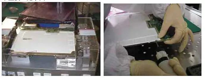
2. Assembly
Assembly is the process of combining the backlight source, screen, control circuit board, and touch screen into a complete display module. Assembly is generally done manually, and skilled technicians are very important here. See the figure below:
In addition to the main processes mentioned above, there are also some auxiliary processes such as: laser cutting lines, electrical testing after cutting, electrical testing after bonding, electrical testing after assembly, microscopic inspection after cutting, microscopic inspection after bonding or automatic optical inspection, shear force peeling tests after IC bonding, tensile peeling tests after FPC bonding, power aging after assembly, packaging and shipment, etc.
5. Conclusion
Although we are not process technicians, we still need to understand related things, because when communicating with other departments or personnel, we can be more adept. When encountering problems, we can consider multiple aspects. If we do not know the relevant knowledge of the process, we will not think of this when encountering problems; therefore, understanding the process is still necessary.
Ending……