Special Edition of ISSCC 2022, Session 10
On the morning of June 10, the 24th session of Doctoral Innovation in “Chip” was held online, featuring the 10th session of the 【ISSCC 2022 Special Edition】.Dr. Zhan Mingtao from Tsinghua University was invited to give a presentation titled “Low-Power High-Speed ADC Design“. The report was simultaneously broadcasted on video platforms such as Tencent Meeting, Kouxiang Academic, and Semiconductor Industry Zongheng. During the Q&A session, the speaker engaged in a lively discussion with online teachers and students on topics such as “Impact of Noise Cancellation Technology on Input Buffers” and “Application of Noise Cancellation Technology in Delta-Sigma ADCs“.
To enrich learning channels and expand learning depth and dimensions,Dr. Zhan Mingtao was invited to provide a detailed written commentary on this report, along with ahighlight reel of the Q&A session,recommended readings, andvideo playback of the report. Let’s revisit the wonderful report of the 24th session through text and video with Dr. Zhan Mingtao!
The latest wireless communication systems such as 5G and WiFi7 have increasingly stringent requirements for the performance and power consumption of ADC. Based on the best energy efficiency metrics of published ADCs at the target sampling rate of GSps, a single-channel ADC for WiFi7 receivers requires several tens of milliwatts of power consumption. If we consider the input buffer and reference voltage buffer of the ADC, the system’s power consumption will be even higher, posing challenges for handheld device applications. Therefore, designing a low-power high-speed analog-to-digital converter is of significant importance. Currently, the mainstream architecture in these applications is the pipeline ADC, whose power consumption bottlenecks mainly come from kT/C noise and the residue amplifier. The fundamental limit of kT/C noise makes it impossible to reduce the sampling capacitance of the ADC, which creates significant difficulties in designing input buffers, reference voltage buffers, and switches. Noise cancellation techniques for kT/C make it possible to break through this limitation. Achieving high-speed, linear, low-noise, low-power, and stable amplifiers presents significant challenges in advanced processes. The ring amplifier (Ringamp) has significant advantages aside from the PVT stability issues. The report introduces its advantages compared to traditional two-stage Miller-OTA. In recent years, pipeline ADCs using Ringamp have demonstrated outstanding energy efficiency metrics, and resolving its stability issues is of great significance. The work of our team at ISSCC 2022 combines these two technologies to solve the stability bias problem of Ringamp while achieving noise cancellation.
Combining kT/C Noise Cancellation with Ringamp
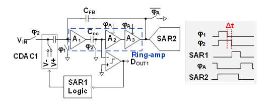
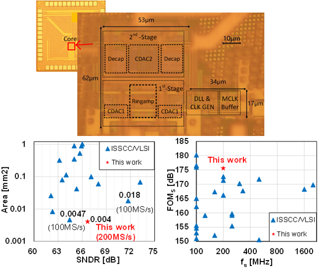
Figure 1: Pipeline ADC combining kT/C and Ringamp
Ringamp Design
The main issue with previous Ringamp structures is that the working currents (pole frequencies) of the second and third stages vary greatly with PVT changes, while using tail current transistors for biasing limits the swing and affects the slew rate, impacting speed. After combining with noise cancellation technology, the noise cancellation capacitor Cnc provides additional degrees of freedom for biasing Ringamp. By using split Cnc, we can bias the NMOS and PMOS of the second stage separately using current mirrors, thus achieving well-defined currents for the second stage, and subsequently using classic Class-AB biasing to obtain well-defined static output currents for the output stage, allowing for excellent control over the operating state of Ringamp.
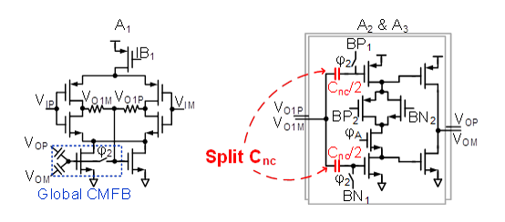
Figure 2: Ringamp with current biasing
Circuit Implementation and Test Results
Q1: Considering the noise of the input buffer, does the noise cancellation technology reduce the power consumption requirements of the input buffer?
The noise within the bandwidth of the input signal cannot be distinguished from the input signal, and this part of the noise cannot be eliminated; however, noise outside the bandwidth of the preamp can be suppressed at the PH2 phase. After adopting noise cancellation technology, due to the significant reduction in sampling capacitance, the front-end circuit may drive the ADC without a buffer, which not only reduces noise sources but also lowers power consumption. Additionally, for high-speed ADCs, increasing current typically alleviates linearity degradation caused by dynamic current extraction from large load capacitance rather than noise issues.
Q2: Can noise cancellation technology be applied in Delta-Sigma ADCs?
Yes, because Delta-Sigma ADCs have oversampling, the input signal frequency is generally far lower than the sampling frequency, and the saturation issue of the preamp is not severe, making it more suitable for adopting noise cancellation technology. In ISSCC 2021, there was an article on Noise Shaping SAR that applied this technology.
Q3: How do you compare noise cancellation technology with continuous-time inputs?
Noise cancellation technology is used in discrete-time systems that require sampling. Using continuous-time inputs avoids aliasing and can reduce noise, but it brings other difficulties to the design of the ADC, such as the challenging delay matching issues in recently developed continuous-time pipeline ADCs.
Q4: How does Ringamp achieve high linearity?
For closed-loop systems, if the swing is sufficient, high linearity can be achieved by increasing open-loop gain. The structure of the Ringamp itself (without cascode transistors) allows for a larger swing, and the multi-stage structure enables high open-loop gain, thus achieving good linearity.
Video Playback