Introduction
In circuit design, level matching is a fundamental requirement, yet it is often overlooked, which can lead to device failures and communication anomalies. In this article, we will reveal how to avoid device failures caused by level mismatches and provide practical design advice to ensure your circuit designs are both efficient and stable.
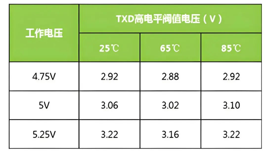
Level matching is a basic requirement in circuit design, but it can easily be overlooked, especially when the specifications of peripherals or chips are not carefully reviewed and designs are based on past experiences, leading to various issues. These problems can often be detected with a little extra scrutiny during the design phase. Below, Case 1 and Case 2 are design errors caused by not thoroughly checking the electrical characteristics of the CAN isolation module, with Case 2 being particularly subtle, involving variations in electrical characteristics at different temperatures:
-
MR6450 connected to a 5V CAN transceiver, operating abnormally;
-
Using a CAN transceiver leads to sporadic operational anomalies.
Level matching is becoming increasingly important in the design of new processor systems, as many processors now feature multiple voltage domains, with some I/O operating at 3.3V and others at 1.8V. Mismatched levels can lead to abnormal operation and even damage to I/O, such as current backflow that can harm I/O ports.
 TTL and CMOS Level Parameter Definitions
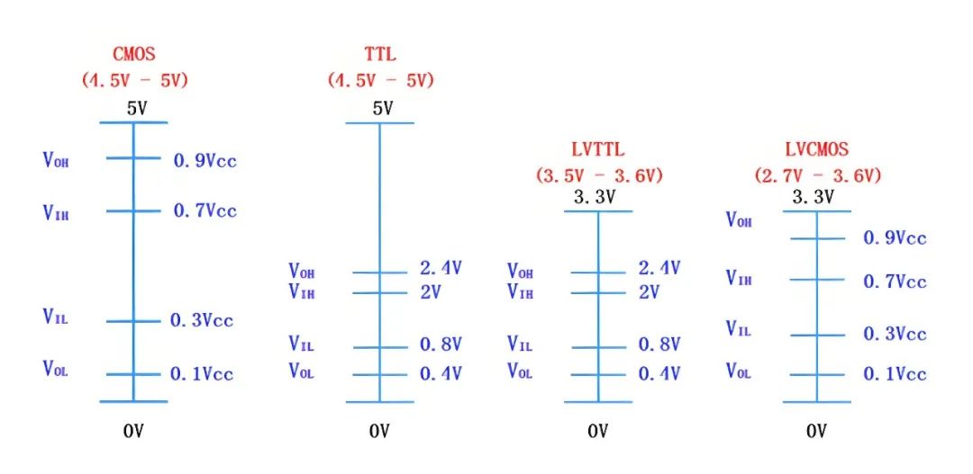
For two devices with different logic levels to achieve reliable signal transmission, the following conditions must be met:
-
The output voltage VOH(MIN) of the driver must be greater than or equal to the input voltage VIH(MIN) of the receiver.
-
The output voltage VOL(MAX) of the driver must be less than or equal to the input voltage VIL(MAX) of the receiver.
-
The output voltage of the driver must not exceed the I/O voltage tolerance of the receiver.
 Case 1: MR6450 UART Pin Connected to 5V Transceiver
The MR6450 core board processor is the HPM6450, whose I/O 3.3V logic level definitions are shown in Figure 2.
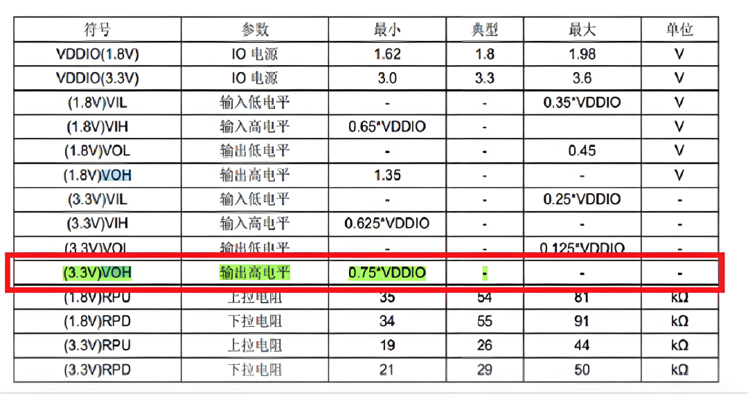
The RS485 module’s 5V logic level definitions are shown in Figure 3.
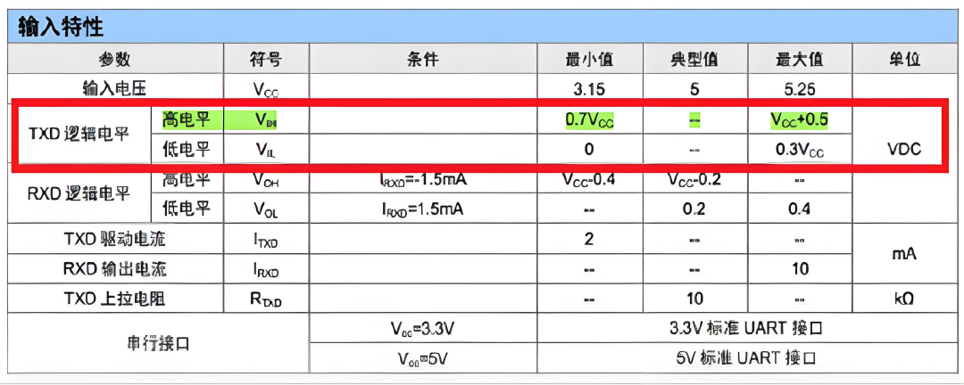
Solution:Select a 3.3V logic level RS485 module, or add a level conversion circuit between the MCU and the module.
 Case 2: CAN Isolation Module Level Mismatch with Processor, Occasional Intermittent Communication Failures
At room temperature, the following signals of the abnormal products were tested: MCU power supply, TXD, CAN differential, and CAN module power supply. The normal waveforms at each point are shown in Figure 4.
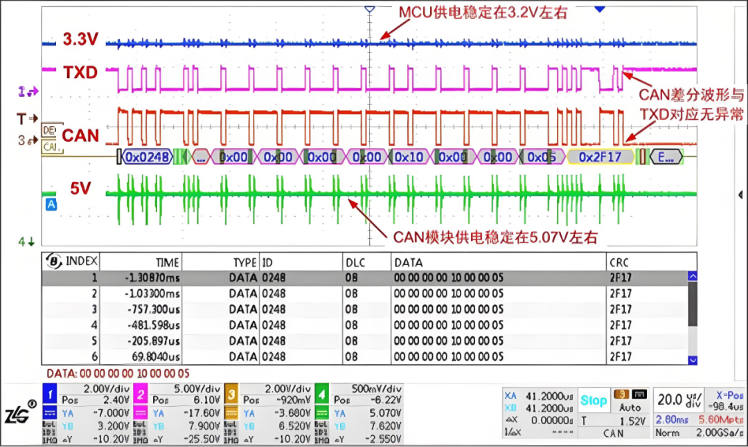
Further high-temperature experiments were conducted. The abnormal products were placed in an oven at 65°C for repeated power-on testing, and the following signals were tested: MCU power supply, TXD, CAN differential, and CAN module power supply. The abnormal waveforms at each point are shown in Figures 5 and 6.
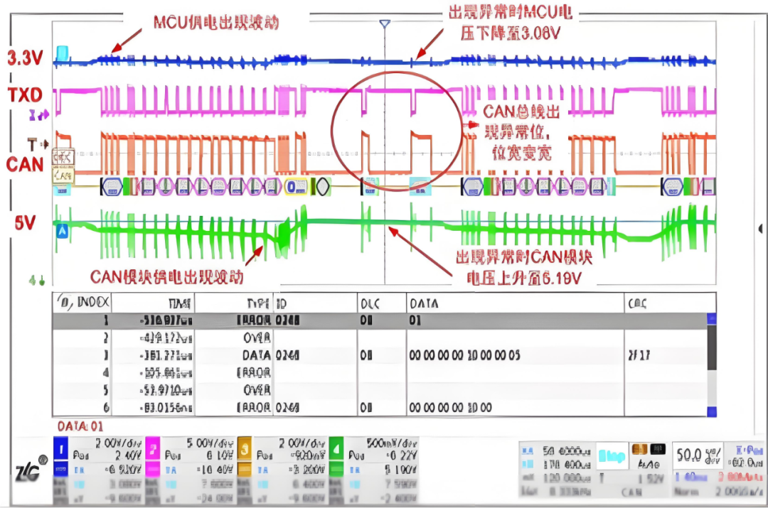
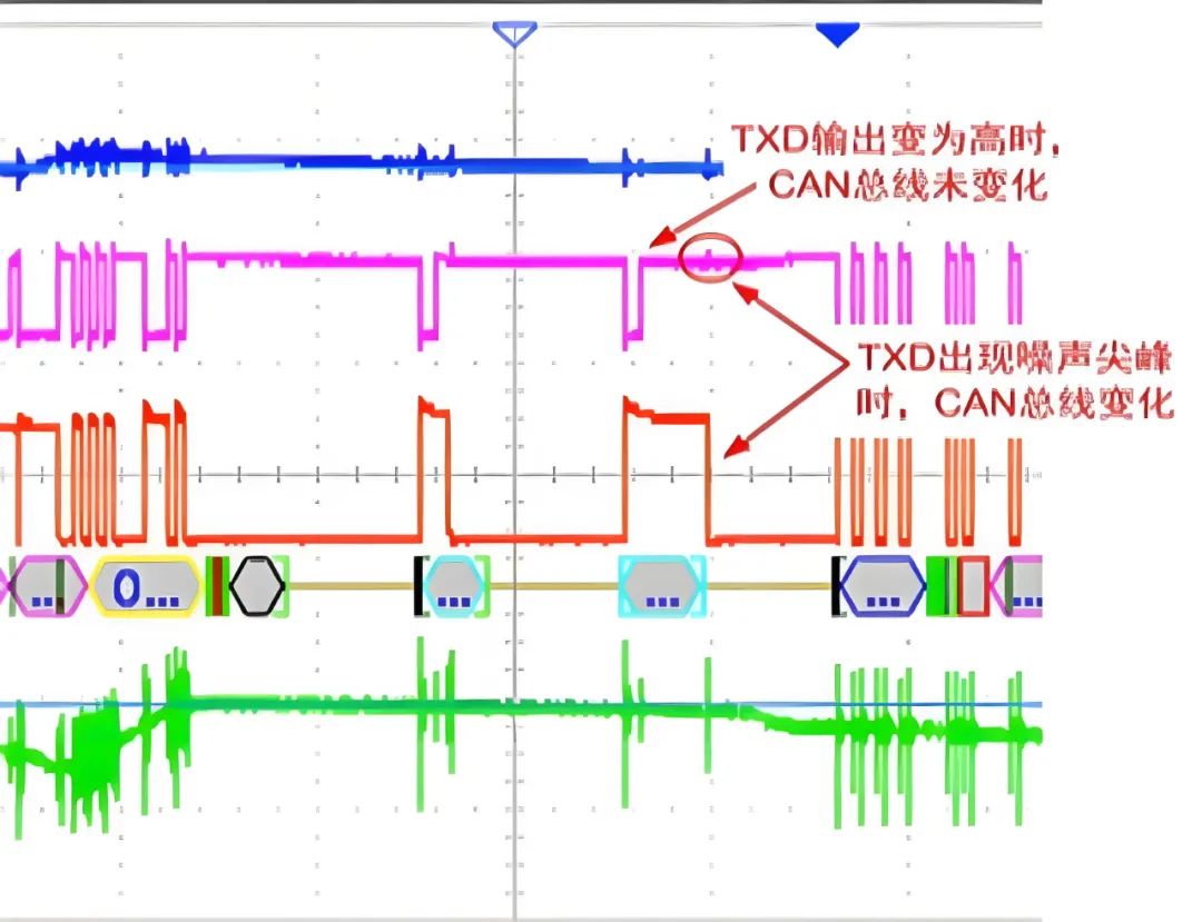
Analysis of the waveform when the CAN bus exhibits abnormal bit width. When the TXD signal transitions from low to high, the CAN bus level remains at the dominant level. Occasionally, noise from the circuit board can cause a slight increase in the TXD level. At this point, the CAN bus level may probabilistically change to the recessive level.
 What to Do If I2C Levels Are Mismatched?
PCA9306 is a bidirectional level shifter that supports I2C and SMBus, allowing level conversion from 1.0V to 3.6V (Vref(1)) to 1.8V to 5.5V (Vbias(ref)(2)). The PCA9306 can operate at two frequencies: 400KHz and 100KHz. The maximum frequency depends on the RC time constant and generally supports >2MHz.
The standard usage circuit for PCA9306 is shown in Figure 8.
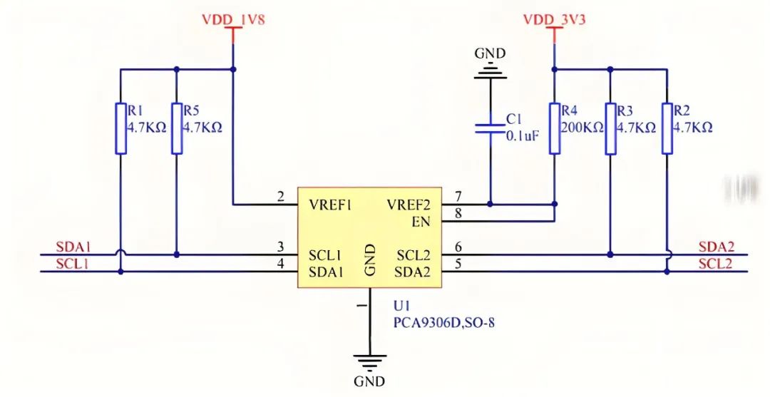
When designing, pay attention to the following points:
-
The voltages VREF1 and VREF2 on both sides cannot be taken arbitrarily, with VREF1 being the low voltage side and VREF2 being the high voltage side;
-
The EN key can be used to control the internal switch’s on and off;
-
The EN and VREF2 pins should be connected together;
-
The value of the pull-up resistor depends on the voltage drop generated when SW is on; refer to the recommended values in the manual.
The circuit shown in Figure 9 is an example of using MOSFETs for level conversion.
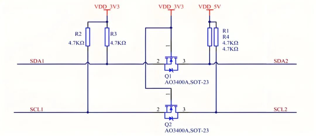
When designing, pay attention to the following points:
-
The low voltage side VDD_3V3 connects to the source of the MOSFET, while the high voltage side VDD_5V connects to the drain of the MOSFET;
-
If converting between other voltage thresholds, such as 3.3V, 2.5V, 1.8V, etc., pay attention to the Vgs turn-on voltage of the MOSFET;
-
This is only suitable for low-speed applications (100/400KHz).
• 15 Serial Ports
• 2 Gigabit Connections
• 4 CANFD Ports
Reference Price: Starting from 49 yuan

Long press to purchase


