Many quantities in reality are analog, such as temperature and pressure. For a microcontroller to understand them, it must first digitize these quantities. AD conversion is the process of converting an analog signal into a digital signal. The AD chip introduced in this book is the ADC0804, an 8-bit parallel AD conversion chip. I won’t copy the detailed principles of AD conversion here, as there is plenty of information available online.
The usage of ADC0804 is much more complicated than the previously used latch 74LS573, mainly because reading and writing data must follow the timing diagram to change the voltage levels, and the chip connections are relatively more complex. Below are the pin definitions:
VIN(+), VIN(-): Input for the analog signal to be measured
DB0~DB7: Output of the measurement result
AGND: Analog signal ground
DGND: Digital signal ground
CLK: Clock signal input
CLKR: External resistor terminal for the internal clock generator. Combined with the CLK terminal, it can generate clock pulses with a frequency of 1/(1.1RC).
CS: Chip select signal, active low
WR: Write signal input, active low to start A/D conversion
RD: Read signal input, active low
INTR: A/D conversion completion signal, active low indicates that the conversion has been completed
VREF/2: Reference level input, determines the quantization unit (this level can be adjusted to fine-tune the final accuracy)
VCC: Power supply input
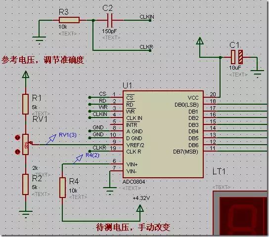
Regarding the clock: If using the internal clock, the official recommendation is to use a 10K resistor and a 150pF capacitor, as shown in the figure above;
Analog ground and digital ground can generally be connected directly to ground. The reference level is around 2.5V; I found that setting it to 2.55 gives relatively accurate results. For the analog signal to be measured, such as voltage, it can be connected as shown in the figure above, with the negative directly connected to ground.
Here, INTR is not used, meaning no interrupts are employed; instead, a delay method is used to wait until the A/D conversion is completed before reading the values from DB0~DB7.
——————————————————————–
Both reading and writing to the chip must follow the chip’s timing. The write timing is as follows:
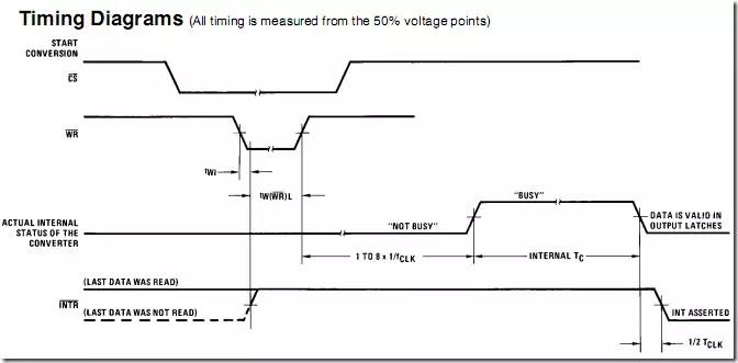
As can be seen, first the chip select signal must be set low, then the write signal goes low, and after it goes high, the chip begins the A/D conversion. Once the conversion is complete, INTR goes low to indicate completion.
The read timing is as follows:
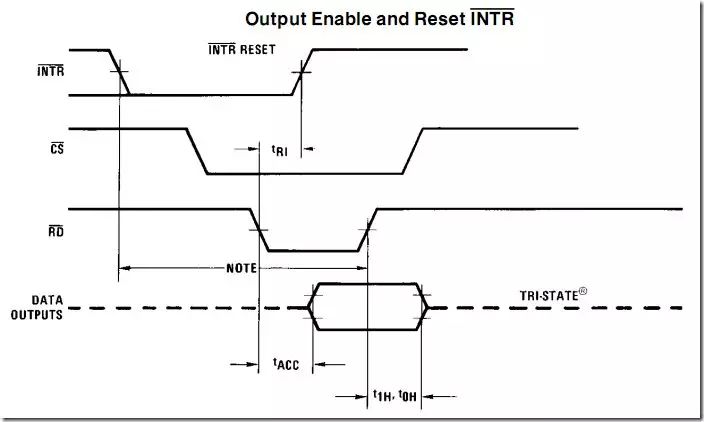
As can be seen, after the conversion is complete, the chip select must be activated, then the read pin goes low and then high to read the data.
Since both reading and writing require the chip select to be active, meaning CS pin must be set low, it can be set low just once.
1void main()
{
uchar val = 0;
// Enable AD chip
ad_cs = 0;
while(1)
{
ad_write = 0; // Set WR pin low
_nop_();
ad_write = 1; // Set WR pin high, complete timing, conversion starts
delay(50); // Wait a bit for conversion to complete, using a 50ms delay since no interrupts are used
P1 = 0xff; // Set all data port bits to 1 to avoid previous data affecting
ad_read = 0; // Set RD pin high
_nop_();
val = P1; // Store data in temporary variable
ad_read = 1; // Set RD pin low
show((val >> 4) * 0.32 + (val & 0x0f) * 0.02); // Convert data to actual voltage based on conversion rules
}
}
The conversion rule is that the high four bits of the 8-bit data correspond to 0.32V per unit, and the low four bits correspond to 0.02V per unit, so the total voltage is:
(val >> 4) * 0.32 + (val & 0x0f) * 0.02
This time, I did not use interrupts and instead used a delay to read, which is somewhat unsatisfactory. If I have time, I will modify the program to use interrupts for notifications.
————————————————————–
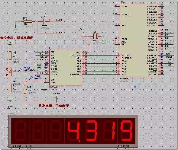
I tried implementing A/D conversion using interrupts, eliminating the need for constant checking, which improved the program’s efficiency. The schematic needs to be slightly modified because it uses external interrupt 0, which corresponds to pin P3.2. This pin was originally connected to the chip select pin of ADC0804, so I need to move the chip select to P3.5 and connect the chip’s INTR to pin P3.2 to trigger the interrupt.