Source: WeChat Official Account “Semiconductor Industry Observation”
In the mid-20th century, the IEEE Electronics and Electrical Engineers Association established an organization called ITRS, which annually published a technology roadmap for the semiconductor field— the ITRS (International Technology Roadmap for Semiconductors). However, in 2017, IEEE stopped updating ITRS and renamed it IRDS, believing that this would provide a more comprehensive reflection of various system-level new technologies.
At the same time, the industry proposed three methods: More Moore, Moore than Moore, and Beyond CMOS, to continuously enhance chip performance. In this article, we have translated the latest version of IRDS 2020, which discusses some roadmap predictions for More Moore. We welcome everyone to read.
Current Technology Status
Most semiconductor devices are digital logic, which requires support for two types of device technology platforms: 1) high-performance logic; 2) low-power/high-density logic. The key considerations for this technology platform are speed, power consumption, density, and cost. The More Moore roadmap provides a reference for the continued expansion of MOSFETs to maintain the historical trend of improving device performance with lower power consumption and cost.
The term “More Moore” refers to the overall approach of continuing CMOS, specifically innovating and researching in areas such as device structure, channel materials, interconnects, high-k metal gates, architectural systems, and manufacturing processes, shrinking along the lines of Moore’s Law.
The following applications drive the demand for More Moore technology in the IRDS:
• High-performance computing — Higher performance under constant power density (heat constraints)
• Mobile computing — Providing more performance and functionality with constant power consumption (battery-limited) and cost
• Autonomous sensing and computing (IoT) — Aiming to reduce leakage and variability
The technology drivers include the following key projects: Logic technologies, Ground rule scaling, Performance boosters, Performance-power-area (PPA) scaling, 3D integration, Memory technologies, DRAM technologies, Flash technologies, Emerging non-volatile memory (NVM) technologies.
The goal of More Moore is to bring PPAC value for node expansion every 2-3 years:
• (P) Performance: Working frequency increases by more than 15% at scaled power supply voltage
• (P) Power: Energy loss per switch reduced by more than 30% at given performance
• (A) Area: Chip area reduced by 30%
• (C) Cost: Wafer cost increases <30% – scaled die cost reduced by 15%.
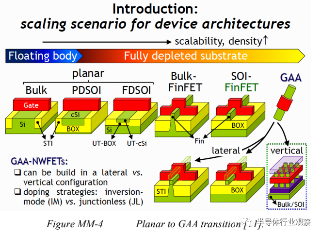
These scaling targets drive significant technological innovations in the industry, including changes in materials and processes, such as high-k gate dielectrics and strain enhancement, as well as new architectures in the near future, such as Gate-All-Around (GAA); alternative high mobility channel materials and new 3D integration schemes allowing heterogeneous stacking/integration. These innovations will be introduced at a rapid pace, making timely understanding, modeling, and implementation into manufacturing critical for the industry.
It is worth noting that cost metrics (15% reduction in die cost) and market rhythm (new products need to be launched every year) are becoming increasingly important in the mobile industry. As applications strictly require all figures of merit (FoM) to be satisfied simultaneously, it is necessary to advance an effective process technology checklist to maintain the limits of certain device architectures, such as pushing the finFET architecture in the next five years.
This approach also helps maintain costs in a risk-reduced manner during the transition from one logic generation to another. As the number of multiple patterning lithography steps increases, the cost of wafer processing becomes increasingly high, making it more challenging. We also need to reduce costs by more than 15% on the same number of transistors, which can only be achieved through advancements in channel materials, device architectures, contact engineering, and device isolation for pitch scaling. The increased process complexity must also be considered in terms of overall die yield. To offset the cost of complexity, design efficiency must be accelerated, further expanding area to achieve die cost ratio goals.
These design-induced scaling factors were also observed in the early work of the ITRS System-Driven Technology Working Group, which were used as calibration factors to match the area scaling trends of the industry. Design scaling factor is now considered one of the key elements of the More Moore technology roadmap.
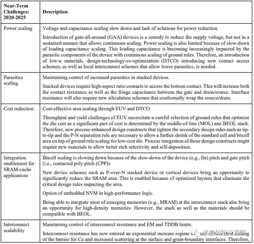
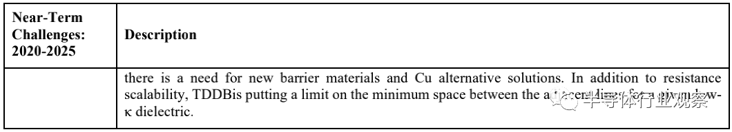
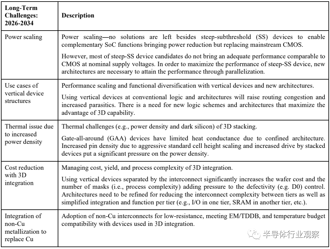
The semiconductor industry’s goal is to continue expanding the overall performance of technology while reducing power consumption and costs. The performance of devices and final chips can be measured in many different ways: higher speed, higher density, lower power consumption, more functionality, etc. Essentially, dimensional scaling has been sufficient to bring the aforementioned performance advantages, but that is no longer the case. Challenges to continuing expansion arise from process, tool, and material performance. We summarize these difficult challenges in Table MM-5 and Table MM-6. These challenges are divided into near-term (2020-2025) and long-term (2026-2034).
As shown in the figure, Table MM-5 presents the near-term challenges.
Table MM-6 illustrates the long-term difficult challenges.
In the More Moore roadmap, we focus on effective solutions to maintain performance and power scaling at scaled dimensions and supply voltages. Ground rule scaling drives die cost reduction. However, this scaling increases parasitics in the total load and results in diminishing returns in performance and power scaling. Therefore, it is necessary to focus on technological scaling solutions while scaling parasitics of devices and interconnects.
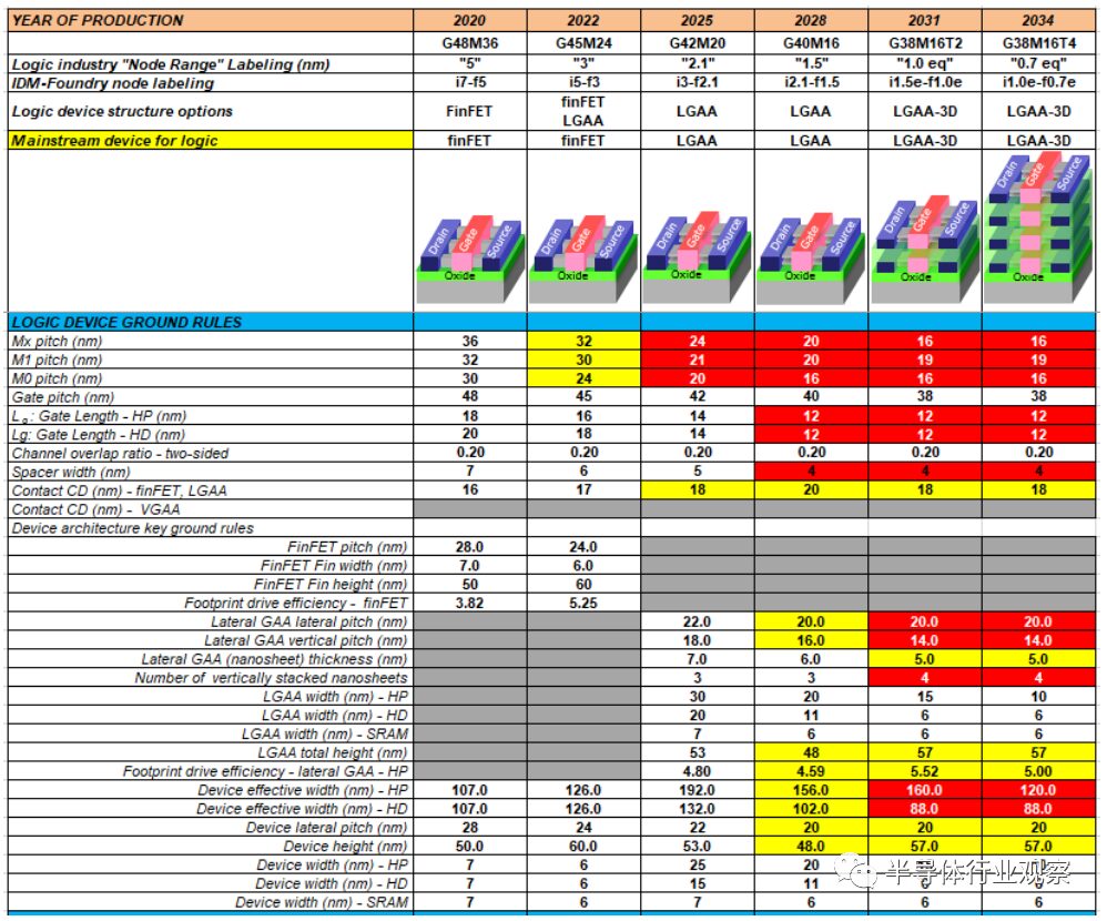
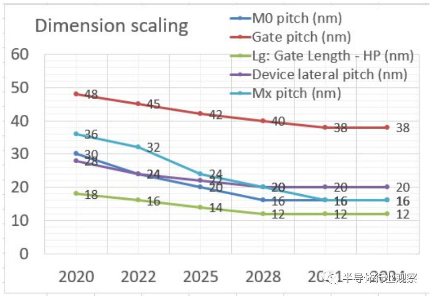
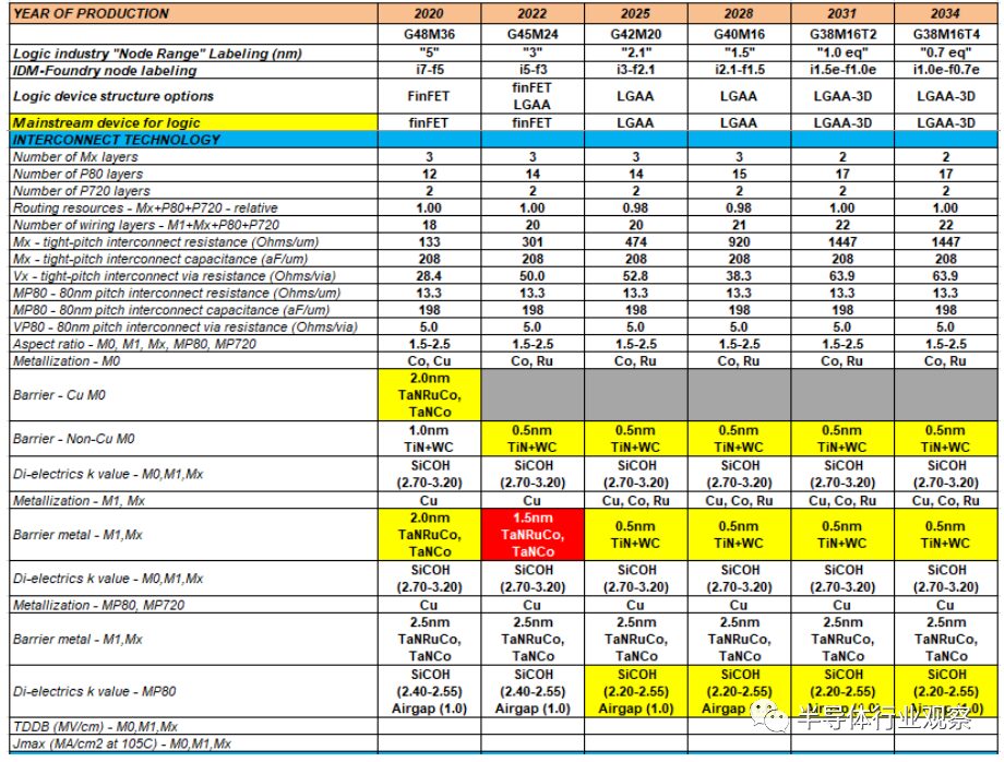
Ground rule scaling also needs to make DTCO structures adaptable to area reduction and tighten the key design rules that limit area scaling. Due to the cost and process complexity of multiple patterning, EUV is used to address the tightly patterned ground rules with fewer process steps. The planned ground rule roadmap and device architecture are shown in Table MM-7. The evolution of ground rules is illustrated in Figure MM-2. There is no consensus on node naming for different foundries and integrated device manufacturers (IDMs); however, the planned rules provide indications of technology capability meeting PPAC requirements. Key parameters in the ground rules include gate pitch, metal pitch, fin pitch, and gate length, which are critical factors for core logic area scaling.
Table MM-7 presents the roadmap for logic device components, PPA, and ground rules.
The acronyms used in the table (in order of appearance): LGAA – lateral gate-all-around-device (GAA), 3DVLSI – fine-pitch 3D logic sequential integration.
Figure MM-2 Projection scaling of key ground rules
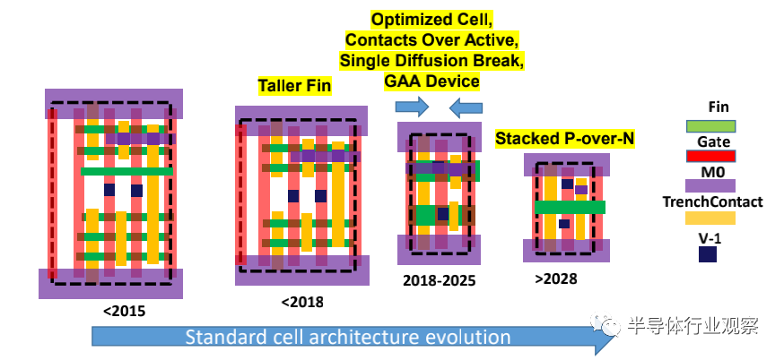
Simply relying on ground rule scaling is insufficient to scale cell height. It is necessary to put design scaling factors into practice. For example, the height of standard cells will be further reduced by scaling the number/width of active devices in standard cells and scaling secondary rules (such as tip-to-tip, extension, P-N separation, and minimum area rules).
Similarly, the width of standard cells can be reduced by focusing on key design rules (e.g., fin end contact) and enabling structures (e.g., active contacts). Additionally, careful selection of contact structures is required to mitigate the risk of increased current density at connections. It is expected that by 2028, P and N devices can be stacked together, further reducing costs. The trend of standard cell scaling is shown in Figure MM-3.
Figure MM-3 Scaling standard cell height and width through fin filling and device stacking
In our view, after 2031, there will be no room for 2D scaling, and three-dimensional VLSI will be necessary for circuits and systems using sequential/stacked integration methods. This is due to the lack of space for contact placement and performance degradation caused by gate pitch scaling and metal pitch scaling.
It is predicted that due to the deterioration of electrostatic effects, physical channel length will saturate around 12nm, while gate pitch will saturate at 38nm to leave enough width (~14nm) for device contacts, providing acceptable parasitics. 3D VLSI is expected to bring PPAC gains for target nodes and pave the way for heterogeneous and/or mixed integration.
The challenge of this 3D integration is how to partition systems to better utilize devices, interconnects, and subsystems (such as memory, analog, and I/O). This is why functional scaling and/or significant architectural changes will be necessary after 2031. This may be the era of Beyond CMOS and specialized technology devices/components, shrinking systems under unit power density and unit volume for high system performance.
In the early years before the 130nm node, transistors followed Dennard scaling, where equivalent oxide thickness (EOT), transistor gate length (Lg), and transistor width (W) were scaled by constant factors to provide latency improvements at constant power density.
Currently, many input parameters can change, while output parameters are complex functions of these input parameters. Other sets of projected parameter values (i.e., different scaling scenarios) can be discovered to achieve the same goals. To maintain low-voltage scaling, recent scaling has focused primarily on other solutions to enhance performance, such as introducing strain in the channel, stress boosters, high-k metal gates, reducing contact resistance, and improving electrostatics. All these are aimed at compensating for gate drive losses while also meeting the low power voltage required for high-performance mobile applications.
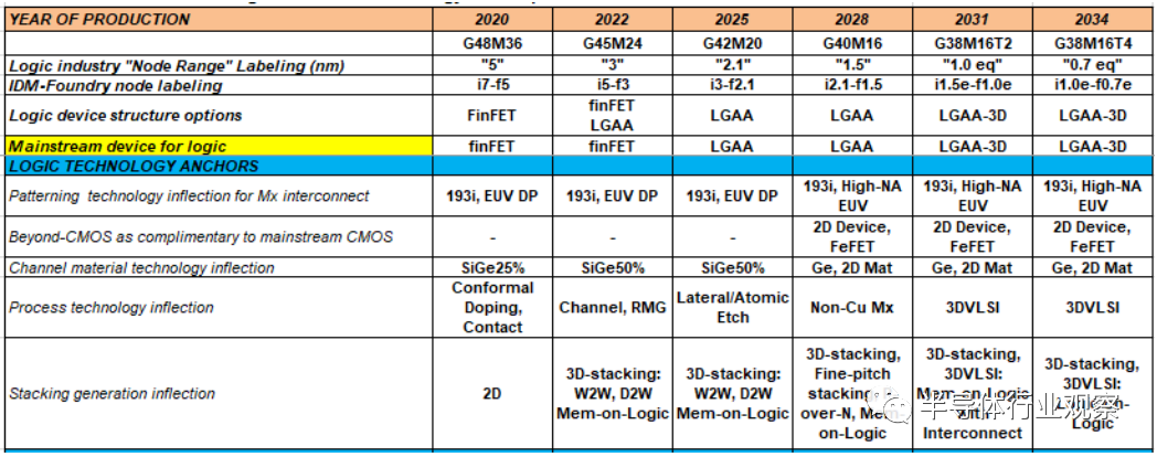
The roadmap overview for device architecture, key modules, and performance boosters is shown in Table MM-8.
Table MM-8 Device roadmap and technology anchoring for More Moore scaling.
FinFET remains a key transistor architecture and appears likely to continue to scale until 2025. Electrostatics and fin population remain two effective solutions for improving performance. Parasitics improvement is expected to continue as a primary means of performance enhancement, resulting from tightening design rules. Parasitics are expected to remain a dominant factor in critical path performance.
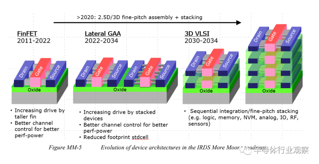
To reduce supply voltage, future transistors must transition to GAA structures such as lateral nanosheets to maintain electrostatic improvements in gate drive. Lateral GAA structures will eventually evolve into a hybrid form with vertical GAA structures to compensate for performance losses due to increased parasitics on tighter pitches and specific SoC functionalities (such as memory selectors).
Sequential integration will allow for monolithic 3D integration stacked on top of each other. The focus of scaling will shift from single-threaded performance improvement to power reduction, then evolve to highly parallel 3D architectures, allowing low Vdd operation and more functionality to be embedded into unit cubic volume.
While device architecture is changing, subsequent modules are also expected to evolve. These may include:
1. Starting substrates, such as silicon-on-insulator (SOI) and strain-relaxation-buffer (SRB);
2. Evolution of channel materials from silicon to SiGe, Ge, and IIIV;
3. Contact modules evolving from silicides to new materials providing lower Schottky barrier height (SBH) and adopting wrap-around contact integration schemes to increase contact surface area.
As previously mentioned, finFET may sustain until 2025. After 2022, the transition to lateral GAA transistors is expected to begin and may include a hybrid form of vertical GAA devices with lateral GAA, potentially 3D hybrid memory-on-logic applications. This situation arises from the limitations of fin width scaling and contact width.
Parasitic capacitance penalty, Weff (effective drive width), and RMG9 (replacement metal gate) integration pose challenges for GAA applications. A trade-off solution may be the EGAA (electrically GAA) architecture, which significantly reduces parasitic capacitance and increases effective width to provide better short-channel control and stronger drive. The evolution planning of transistor architectures is illustrated in Figures MM-5 and MM-5.
Bulk silicon will remain the mainstream substrate, while silicon-on-insulator (SOI) and SRB will be used to support better isolation (e.g., RF integration) and high mobility channels for defect-free integration.
We know that high mobility materials like Ge and III-V materials hold promise for increasing drive current by increasing inherent mobility by an order of magnitude. As gate length scales, the impact of mobility on drain current becomes limited due to velocity saturation.
On the other hand, as gate length continues to shrink, carrier transport becomes ballistic. This causes the carrier speed (also known as “injection speed”) to increase with increased mobility, leading to an increase in drain current. However, for high mobility devices, low effective mass can actually lead to high tunneling currents at higher supply voltages. This may degrade the effective performance of III-V devices post short-channel work function tuning (e.g., threshold voltage increase) to reduce leakage current (Ioff) to compensate for tunneling current.
Another issue to consider for high mobility channels is the lower density of states. Current is proportional to the product of drift velocity and carrier concentration in the channel. This necessitates the proper selection of gate length (Lg), supply voltage (Vdd), and device structure to maximize this product, and the selection of these parameters will differ depending on the type of channel material used. All of this needs to be addressed holistically.
High mobility channels are likely to be used for continuous integration to synergistically integrate high-speed I/Os, RF (such as 5G and beyond), and photonics.
In the past decade, strain engineering has been one of the most effective solutions, as seen in the 32nm node and earlier. However, the effects of these stressors may not intuitively carry over to new nodes. As gate pitch narrows, source-drain epitaxial (S/D EPI) contacts and SiGe on SRB remain effective boosters with more than double the mobility of high mobility channel materials. Engineers have successfully demonstrated PMOS SiGe channels and NMOS strain Si channels on 7nm CMOS platforms using SRB.
On the other hand, SRB or S/D stress sources may not have an effect on channel stress in vertical devices. Other strain engineering techniques include gate stressors and ground plane stressors.
Interconnects and 3D Heterogeneous Integration
For the future of chips, interconnects are also an important aspect, and the most difficult challenge in interconnects is introducing new materials that meet wire conductivity requirements, reduce dielectric constant, and satisfy reliability requirements. For conductivity, it is necessary to reduce the impact of size effects on the interconnect structure. Size control is a key challenge facing today’s and future generations of interconnect technologies, and the resulting etching challenges involve forming precise channel and via structures in low-k dielectric materials to minimize RC variations.
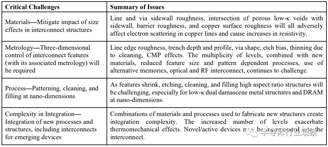
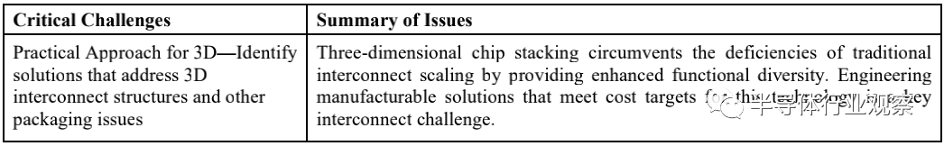
To achieve maximum performance, interconnect structures cannot tolerate profile variations without incurring undesirable RC degradation. These size control requirements pose new demands for high-throughput imaging metrology to measure high aspect ratio structures. New metrology techniques are also needed to monitor adhesion and defects online. The need for larger wafers and to limit testing wafers will drive the adoption of more process control technologies in the field. Table MM-12 highlights and distinguishes the most significant challenges, while Table MM-13 shows the interconnect scaling roadmap.
Table MM-12 Interconnect challenges
Table MM-13 Interconnect scaling roadmap
At least until 2025, copper (Cu) is expected to remain the preferred solution for interconnect metals, while non-copper solutions (such as Co and Ru) are expected to be used for local interconnects (M0). On the other hand, due to limitations of electromigration, local interconnects (middle-of-line: MOL), M1, and Mx levels will use non-copper solutions like cobalt (Co), especially for vias, as it has a better integration window for filling narrow trenches while having lower resistance than copper at scaled sizes.
Copper wiring and line barrier materials must prevent copper diffusion into adjacent dielectrics, but must also form appropriate, high-quality interfaces with copper to limit vacancy diffusion and achieve acceptable electromigration lifetimes. Ta(N) is a well-known industry solution. Mn(N) has also received significant attention in recent years. For new materials, self-assembled monolayers (SAMs) are one of the candidate materials.
Meanwhile, 3D heterogeneous integration has also become a focus.
It is well known that each generation of logic nodes needs to add new functions to maintain unit prices (to keep profit margins). Due to the following challenges, this has become more difficult:
• Fewer co-integrated functions on board/system
• Each function’s dedicated heterogeneous core and the dedicated performance improvement requirements for each core
• The high cost of package external memory and logic co-integration, and incompatibility with baseline CMOS technology (which may require wafer/chip-level stacking)
So far, die cost reduction has been achieved through synchronous scaling of gate pitch, metal pitch, and cell height. This situation is expected to continue until 2028. In cell and physical design, three-dimensional devices (such as finFET and lateral GAA) and DTCO structures may pursue cell height scaling. However, this scaling path is expected to face greater challenges due to the reduced electrical/system benefits and the diminishing area reduction at the SoC level.
Therefore, it is necessary to seek 3D integration, such as device-over-device stacking, fine-pitch layer transfer, and/or monolithic 3D (or sequential integration). These pursuits will maintain system performance and power gains while potentially retaining cost advantages, such as processing expensive non-scaled components elsewhere and using the most suitable technology for each layer’s functionality.
3DVLSI can be wired at the gate level or transistor level. 3DVLSI provides the possibility of stacked layers, achieving high-density contacts at the layer level (up to millions of vias per square millimeter). Gate-level partitioning allows for IC performance gains due to reduced wire lengths while achieving independent optimization of both types of transistors (custom implementation of channel material/substrate orientation/channel and enhanced source/drain strain, etc.) by stacking nFETs on pFETs (or vice versa), while reducing process complexity compared to planar co-integration, such as stacking III-V nFETs over SiGe pFETs.
These high mobility transistors are well-suited for 3DVLSI due to their low process temperatures. High-density 3DVLSI can also enable applications for heterogeneous co-integration with high-density 3D vias, such as CMOS for gas sensing or highly miniaturized imagers. Integrating device-over-device stacking (e.g., P devices over N devices) to decouple channel engineering (e.g., Ge channel for PMOS) for better performance is a significant development momentum.
To address the transition from 2D to 3DVLSI, the roadmap predicts the following generations:
(1) Die-to-wafer and wafer-to-wafer stacking:
Method: Fine-pitch dielectric/hybrid bonding and/or flip-chip assembly
Opportunity: Reduce material lists on systems, heterogeneous integration, high bandwidth and low latency memory in logic
Challenge: Design/architecture partitioning
(2) Device-over-device (e.g., P-over-N stacking)
Method: Sequential integration
Opportunity: Reduce 2D footprint of standard cells and/or bit cells
Challenge: Minimizing interconnect overhead is key to achieving low costs between N&P
(3) Adding logic 3D SRAM and/or MRAM stacks (embedded/stacked)
Method: Sequential integration and/or wafer transfer
Opportunity: 2D area gain, better connection between logic and memory, yielding system latency gains.
Challenge: If using stacking methods, address the thermal budget of lower layer interconnects, revisit cache hierarchy and application requirements, power and clock distribution
(4) Adding analog and I/O methods: Sequential integration and/or wafer transfer
Opportunity: Provide designers with more freedom, allowing integration of high mobility channels, pushing non-scaled components to another layer, IP reuse, scalability
Challenge: Thermal budget, reliability requirements, power and clock distribution
(5) True-3D VLSI: Cluster function stacks
Method: Sequential integration and/or wafer transfer
Opportunity: Complementary functions rather than CMOS replacements, such as neuromorphic, high-bandwidth memory or pure logic applications integrated into new data flow schemes. Application examples include image recognition in neuromorphic structures, wide I/O sensor interfaces (e.g., DNA sequencing, molecular analysis), and highly parallel memory logic computation.
Challenge: Architectural applications that can leverage low energy, low frequency, and highly parallel interfaces, mapping applications to non-Von Neumann architectures.
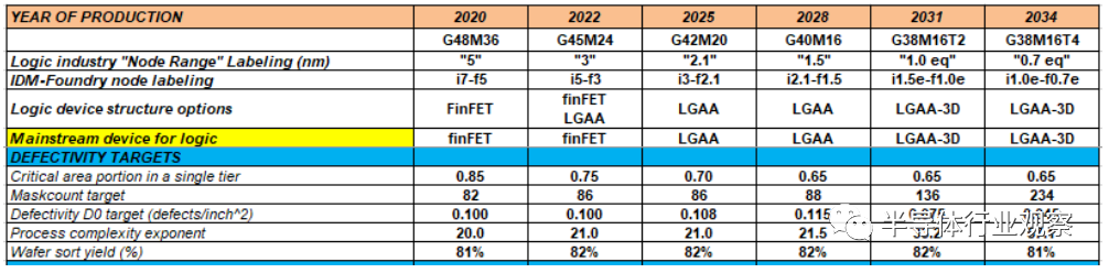
More Moore scaling requires increasing the number of metallization layers; therefore, without advancements in patterning technology, the number of masks will need to increase. The transition from 193i lithography to EUV is expected to potentially save masks. However, due to the increasing demand for masks for metallization and for FEOL and MOL integration for 3D integration, the number of masks is expected to rise post-2031. This, in turn, will increase process complexity, thereby increasing defect (D0) demand. The D0 levels required by 2034 are expected to decrease by 2.2 times to maintain the yield of 80mm2 die under control.
Table MM-15 Defect rate (D0) requirements for 80mm2 die.
Memory Technology Must Keep Pace
CMOS logic and memory together constitute the main part of semiconductor device production. After discussing logic devices, we need to consider memory.
As is well known, the types of memory include DRAM and non-volatile memory (NVM). We focus on commercial, standalone chips as these tend to drive memory technology. However, embedded memory chips are expected to follow the same trends as commercial memory chips, usually with a certain lag. For both DRAM and NVM, detailed technical requirements and potential solutions have been considered.
For DRAM, the main goal is to continue to shrink the footprint of the 1T-1C cell, reaching the practical limit of 4F2. The challenge is the vertical transistor structure, and high-k dielectrics improve capacitance density while maintaining low leakage. From the current technology perspective, the technical requirements for DRAM are becoming increasingly challenging as scaling progresses. In recent years, many new technologies have been introduced in DRAM, such as 193 nm ArF immersion high-sodium lithography technology, improvements in cell FET technology including FinFETs, buried word lines, and cell FET, among others.
As the storage capacitor in DRAM becomes physically smaller, EOT (equivalent oxide thickness) must decrease sharply to maintain sufficient storage capacitance. To measure EOT, dielectric materials with high relative permittivity (κ) are required. Therefore, we adopt MIM (metal-insulator-metal) capacitors, selecting high-k (ZrO2/Al2O/ZrO2) materials. The development and improvement of this material have continued to the release of 20nm HP and ultra-high-k (perovskite κ > 50 ~ 100) materials. Additionally, the physical thickness of high-k insulators should be scaled proportionally to accommodate minimum feature sizes. Therefore, the three-dimensional structure of capacitors will change from cylindrical to columnar.
On the other hand, as the peripheral CMOS devices scale, the process steps required for these devices necessitate low-temperature processing. This poses a challenge for typically constructing DRAM cell processes after the formation of CMOS devices, thus limiting them to low-temperature processing. The requirements for DRAM peripheral devices can relax Ioff but require more LSTP (Ion of low standby power) devices. However, future high-k metal gates are necessary to maintain performance.
Another important topic is the transition from 6F2 to 4F2 cells. Maintaining cost trends becomes impossible as half-pitch scaling becomes extremely challenging. The most promising way to maintain cost trends is to change the scaling of the cell size factor (a = [DRAM cell size]/[DRAM half pitch]]2). Currently, 6F2 (a = 6) is the most common. For example, vertical cell transistors are needed, but there are still some challenges.
In summary, maintaining sufficient storage capacitance and adequate cell transistor performance is necessary to sustain time characteristics in the future. To continue scaling DRAM devices and achieve greater product capacity, their difficulty index continues to increase. Moreover, if the efficiency of cost scaling worsens compared to the introduction of new technologies, DRAM scaling may stop, adopting 3D cell stacking structures or new DRAM concepts. Discussions have been held regarding 3D cell stacking and new concept DRAM, but there is no clear path for further extending 2D DRAM.
Beyond DRAM, there are several memory technologies that share a common feature—non-volatility. Depending on the application, the requirements and challenges vary, from RFID requiring only Kb storage to high-density storage in chips of hundreds of Gb. Non-volatile memories can be divided into two major categories—flash memory (NAND flash and NOR flash) and non-charge storage-based memories. Non-volatile memory is essentially ubiquitous, and many applications using embedded memory typically do not require cutting-edge technology nodes. The More Moore non-volatile memory table only tracks memory challenges and potential solutions for leading standalone components.
Flash memory is based on simple single-transistor (1T) cells, where the transistor serves both as the access (or cell selection) device and the storage node. Currently, flash memory serves over 99% of applications.
When the number of electrons stored reaches statistical limits, even if devices can be further scaled and smaller cells achieved, the threshold voltage distribution of all devices in the storage array becomes uncontrollable, and the logic state becomes unpredictable. Therefore, it is impossible to indefinitely increase storage density by continuously scaling charge-based devices. However, effective density increases can continue through vertical stacking of storage layers.
The economic viability of completing one device layer and then stacking another device layer is questionable. As shown in Figure MM-12, the bit cost begins to rise after stacking multiple device layers. Moreover, yield losses due to increased interconnects and complex processing may further reduce the bit cost-effectiveness of this 3D stacking.
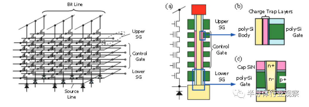
In 2007, a new manufacturing method was proposed that significantly simplified process steps. This method allows for the production of 3D stacked devices with just a few steps without repeated processing, providing a new low-cost scaling path for NAND flash. Figure MM-12 illustrates one such method. This architecture was initially referred to as bitcost-scalable (BiCS), which turns NAND strings from a horizontal position to a vertical position by 90 degrees. The word line (WL) remains in the horizontal plane. As shown in Figure MM-12, this type of 3D method is much more economical than stacking complete devices, and the cost-effectiveness does not saturate at relatively high layer counts.
 Since 2007, many architectures based on the BiCS concept have been proposed, some of which use floating gates instead of charge trapping storage architectures, and these technologies have entered mass production in the past 2-3 years. Overall, all 3D NAND methods adopt a larger area occupancy strategy than traditional 2D NAND. Compared to the minimal 2D NAND of ~15nm, the x- and y-dimensions of 3D NAND (equivalent to 2D cell sizes) are in the range of 100nm and above. The larger “cell size” is achieved by stacking a large number of storage layers to achieve competitive packaging density.
The economic benefits of 3D NAND are further complicated by its complex and unique manufacturing requirements. While larger cell sizes seem to relax the requirements for fine-line lithography, achieving high data rates necessitates using larger page sizes, which in turn translates into fine line spacing for bit lines and metal lines. Therefore, even with large cell sizes, metal lines still require approximately 20nm of half-pitch, which can only be achieved through 193i lithography and dual-patterning. Deep hole etching is challenging and slow, and etching throughput is typically low. Depositing multiple dielectric and/or polysilicon layers, as well as metrology for multilayer films and deep holes, is a challenge. All these translate into substantial investments in new devices and footprint, as well as new challenges for wafer flow and yield.
How many layers can flash memory ultimately stack? This seems to be an unknown number. Because there appears to be no strict physical limit on layer stacking. However, we recognize that after a certain aspect ratio (perhaps 100:1?), the etching stop phenomenon may occur, where ions in the reactive ion etching process cannot propagate downward due to electrostatic charges on the sidewalls, potentially limiting how many layers can be etched in one operation.
However, this issue can be circumvented by stacking fewer layers and etching and stacking more layers (at higher costs). Stacking many layers may induce high stress, causing wafer warping, although this does not seem to be an insurmountable physical limit with careful design. Even at 200 layers (each layer about 50nm), the total stacking height of about 10μm is still within the same range as the 10-15 metal layers of logic ICs. This layer thickness does not significantly affect the thickness of the die (so far, the thinnest thickness is about 40μm).
However, at 1000 layers, the total layer thickness may lead to a thickness of the die that does not comply with the form factor required for stacking multiple dies (e.g., 16 or 32) in thin packages. Now that flash memory has reached over 170 layers, we consider that 256 layers in the future is also possible.
When stacking more layers proves too difficult, the area x-y may ultimately begin to shrink. However, this trend is not guaranteed. If the aspect ratio of the holes is a limitation, shrinking the footprint will not reduce the ratio, thus providing no help. Additionally, the larger cell sizes seem to at least partially contribute to the better performance (speed and cycle reliability) of 3D NAND compared to compact 2D NAND. Whether x-y scaling can still provide such performance remains unclear. New innovations or more robust emerging memories may be needed to further reduce bit costs.
As the scaling of 2D NAND Flash is limited by the statistical fluctuations caused by insufficient stored charge, several unconventional non-volatile memories (ferroelectric or FeRAM, magnetic or MRAM, phase change or PCRAM, resistive or ReRAM) are being developed and forming a category commonly referred to as “emerging” memories.
Even if 2D NAND is replaced by 3D NAND (no longer troubled by insufficient electron numbers), certain characteristics of emerging memories based on non-charge storage (such as low voltage operation or random access) are attractive for various applications. Therefore, the continued development of these emerging memories often features two-terminal structures (e.g., resistors or capacitors), making them difficult to coexist as cell selection devices. Memory cells are typically combined in forms such as 1T-1C, 1T-1R, or 1D-1R.
FeRAM devices achieve non-volatility by switching and detecting the polarization state of ferroelectric capacitors. To read the stored state, it is necessary to track the hysteresis loop of the ferroelectric capacitor, which destroys the stored data, and it must be written back after reading (destructive read, like DRAM). Finding ferroelectric and electrode materials that can provide sufficient polarization changes while offering necessary stability over extended operating cycles is a challenge. Many ferroelectric materials do not complement conventional CMOS manufacturing materials and can degrade under standard CMOS process conditions.
FeRAM is fast, low-power, and low-voltage, making it suitable for RFID, smart cards, ID cards, and other embedded applications. However, the processing difficulty limits its widespread adoption. Recently, HfO2-based ferroelectric FETs have been proposed, where the ferroelectric acts to change the FET’s Vt, forming a 1T cell similar to flash memory. If matured, this new memory could become a low-power, very fast flash-like memory.
MRAM (Magnetic RAM) devices use magnetic tunnel junctions (MTJ) as storage elements. MTJ cells consist of two ferromagnetic materials separated by a thin insulating layer that acts as a tunneling barrier. When one layer’s magnetic moment aligns (or opposes) the magnetic moment of the other layer, the effective resistance of the current flowing through the MTJ changes. The magnitude of the tunneling current can indicate whether a 1 or 0 is stored.
Field-switching MRAM may be the closest to an ideal “universal memory” as it is non-volatile, fast, and can cycle indefinitely. Thus, it can serve as both NVM and SRAM and DRAM. However, generating magnetic fields in integrated circuits is both challenging and inefficient. However, field-switching MTJ MRAM has been successfully produced. However, the magnetic field required for switching increases with the scaling of storage elements, while electromigration limits the current density available to generate higher H fields.
Therefore, it is expected that field-switching MTJ MRAM is unlikely to scale below the 65nm node. Recent STT (spin-transfer torque) MRAM may present new opportunities.
With the rapid development of NAND flash technology and the introduction of 3D NAND technology expected to continue achieving equal scaling, the hope for STT-MRAM to replace NAND seems distant. However, its SRAM-like performance and much smaller memory footprint than traditional 6T-SRAM has generated significant interest in SRAM applications, particularly in mobile devices where high cycle endurance is not required. Thus, STT-MRAM is currently mainly viewed as an embedded memory and is not tracked in the standalone NVM table.
STT-MRAM is not only an alternative to embedded SRAM but also to embedded Flash (NOR). This could be particularly interesting for IoT applications, as low power consumption is paramount. On the other hand, for other embedded system applications requiring higher memory density, NOR Flash is expected to continue to dominate as it still offers greater cost-effectiveness. Additionally, flash memory has established the capability to endure the PCB soldering process (~ 250°C) without losing its loaded code, while many emerging memories have yet to demonstrate feasibility.
Other technologies such as PCRAM, Crosspoint memory, and ReRAM are also worth attention, but due to space limitations, we will not introduce them one by one.
Since 2007, many architectures based on the BiCS concept have been proposed, some of which use floating gates instead of charge trapping storage architectures, and these technologies have entered mass production in the past 2-3 years. Overall, all 3D NAND methods adopt a larger area occupancy strategy than traditional 2D NAND. Compared to the minimal 2D NAND of ~15nm, the x- and y-dimensions of 3D NAND (equivalent to 2D cell sizes) are in the range of 100nm and above. The larger “cell size” is achieved by stacking a large number of storage layers to achieve competitive packaging density.
The economic benefits of 3D NAND are further complicated by its complex and unique manufacturing requirements. While larger cell sizes seem to relax the requirements for fine-line lithography, achieving high data rates necessitates using larger page sizes, which in turn translates into fine line spacing for bit lines and metal lines. Therefore, even with large cell sizes, metal lines still require approximately 20nm of half-pitch, which can only be achieved through 193i lithography and dual-patterning. Deep hole etching is challenging and slow, and etching throughput is typically low. Depositing multiple dielectric and/or polysilicon layers, as well as metrology for multilayer films and deep holes, is a challenge. All these translate into substantial investments in new devices and footprint, as well as new challenges for wafer flow and yield.
How many layers can flash memory ultimately stack? This seems to be an unknown number. Because there appears to be no strict physical limit on layer stacking. However, we recognize that after a certain aspect ratio (perhaps 100:1?), the etching stop phenomenon may occur, where ions in the reactive ion etching process cannot propagate downward due to electrostatic charges on the sidewalls, potentially limiting how many layers can be etched in one operation.
However, this issue can be circumvented by stacking fewer layers and etching and stacking more layers (at higher costs). Stacking many layers may induce high stress, causing wafer warping, although this does not seem to be an insurmountable physical limit with careful design. Even at 200 layers (each layer about 50nm), the total stacking height of about 10μm is still within the same range as the 10-15 metal layers of logic ICs. This layer thickness does not significantly affect the thickness of the die (so far, the thinnest thickness is about 40μm).
However, at 1000 layers, the total layer thickness may lead to a thickness of the die that does not comply with the form factor required for stacking multiple dies (e.g., 16 or 32) in thin packages. Now that flash memory has reached over 170 layers, we consider that 256 layers in the future is also possible.
When stacking more layers proves too difficult, the area x-y may ultimately begin to shrink. However, this trend is not guaranteed. If the aspect ratio of the holes is a limitation, shrinking the footprint will not reduce the ratio, thus providing no help. Additionally, the larger cell sizes seem to at least partially contribute to the better performance (speed and cycle reliability) of 3D NAND compared to compact 2D NAND. Whether x-y scaling can still provide such performance remains unclear. New innovations or more robust emerging memories may be needed to further reduce bit costs.
As the scaling of 2D NAND Flash is limited by the statistical fluctuations caused by insufficient stored charge, several unconventional non-volatile memories (ferroelectric or FeRAM, magnetic or MRAM, phase change or PCRAM, resistive or ReRAM) are being developed and forming a category commonly referred to as “emerging” memories.
Even if 2D NAND is replaced by 3D NAND (no longer troubled by insufficient electron numbers), certain characteristics of emerging memories based on non-charge storage (such as low voltage operation or random access) are attractive for various applications. Therefore, the continued development of these emerging memories often features two-terminal structures (e.g., resistors or capacitors), making them difficult to coexist as cell selection devices. Memory cells are typically combined in forms such as 1T-1C, 1T-1R, or 1D-1R.
FeRAM devices achieve non-volatility by switching and detecting the polarization state of ferroelectric capacitors. To read the stored state, it is necessary to track the hysteresis loop of the ferroelectric capacitor, which destroys the stored data, and it must be written back after reading (destructive read, like DRAM). Finding ferroelectric and electrode materials that can provide sufficient polarization changes while offering necessary stability over extended operating cycles is a challenge. Many ferroelectric materials do not complement conventional CMOS manufacturing materials and can degrade under standard CMOS process conditions.
FeRAM is fast, low-power, and low-voltage, making it suitable for RFID, smart cards, ID cards, and other embedded applications. However, the processing difficulty limits its widespread adoption. Recently, HfO2-based ferroelectric FETs have been proposed, where the ferroelectric acts to change the FET’s Vt, forming a 1T cell similar to flash memory. If matured, this new memory could become a low-power, very fast flash-like memory.
MRAM (Magnetic RAM) devices use magnetic tunnel junctions (MTJ) as storage elements. MTJ cells consist of two ferromagnetic materials separated by a thin insulating layer that acts as a tunneling barrier. When one layer’s magnetic moment aligns (or opposes) the magnetic moment of the other layer, the effective resistance of the current flowing through the MTJ changes. The magnitude of the tunneling current can indicate whether a 1 or 0 is stored.
Field-switching MRAM may be the closest to an ideal “universal memory” as it is non-volatile, fast, and can cycle indefinitely. Thus, it can serve as both NVM and SRAM and DRAM. However, generating magnetic fields in integrated circuits is both challenging and inefficient. However, field-switching MTJ MRAM has been successfully produced. However, the magnetic field required for switching increases with the scaling of storage elements, while electromigration limits the current density available to generate higher H fields.
Therefore, it is expected that field-switching MTJ MRAM is unlikely to scale below the 65nm node. Recent STT (spin-transfer torque) MRAM may present new opportunities.
With the rapid development of NAND flash technology and the introduction of 3D NAND technology expected to continue achieving equal scaling, the hope for STT-MRAM to replace NAND seems distant. However, its SRAM-like performance and much smaller memory footprint than traditional 6T-SRAM has generated significant interest in SRAM applications, particularly in mobile devices where high cycle endurance is not required. Thus, STT-MRAM is currently mainly viewed as an embedded memory and is not tracked in the standalone NVM table.
STT-MRAM is not only an alternative to embedded SRAM but also to embedded Flash (NOR). This could be particularly interesting for IoT applications, as low power consumption is paramount. On the other hand, for other embedded system applications requiring higher memory density, NOR Flash is expected to continue to dominate as it still offers greater cost-effectiveness. Additionally, flash memory has established the capability to endure the PCB soldering process (~ 250°C) without losing its loaded code, while many emerging memories have yet to demonstrate feasibility.
Other technologies such as PCRAM, Crosspoint memory, and ReRAM are also worth attention, but due to space limitations, we will not introduce them one by one.
Editor: Southern Cat