Learning STM32 Minimum System Board Circuit Knowledge
The minimum system of a microcontroller refers to the system that can work with the least amount of circuitry, usually including: power circuit, clock circuit, reset circuit, debugging/download circuit, and for STM32, a boot selection circuit is also needed. In short, if you don’t understand the circuit at first, just copy someone else’s circuit and piece it together yourself. The following is the classic circuit schematic of STM32C8T6. 
Table of Contents
-
Learning STM32 Minimum System Board Circuit Knowledge
-
1. Power Conversion Circuit
-
2. JTAG/SWD Debug Interface Circuit
-
3. Clock Circuit
-
4. Reset Circuit
<span>Note: The following is the main content of this article, the examples below can be used for reference.</span>
1. Power Conversion Circuit
The development board usually uses USB power supply, and USB is generally 5V, so it is necessary to convert 5V to 3.3V, which can be achieved using the TPS73633 or AMS1117 power chip. First, design the power entry part. Currently, most development boards use USB’s 5V power supply, so we also use a USB interface for power supply in this design. Therefore, our power interface adopts a 5Pin mini surface-mounted USB, bringing 5V power into the development board for use. The circuit diagram is as follows, pin 1 is the positive power supply, pin 5 is the negative power supply, and the series diode is to protect our development board from being burned due to incorrect polarity of individual connecting wires. Protection circuits must be considered when designing any circuits, and this is something everyone should pay attention to when designing in the future. This way, we can use the connecting wire to bring 5V USB power into the development board.
 Next is the power circuit. The operating voltage of STM32 is DC3.3V, so we need a chip that can convert a voltage greater than 3.3V to a stable 3.3V voltage, which can be achieved using the TPS73633 or AMS1117 power chip.
  The following is a description of the TPS73633 chip. TPS73633DBVR is a low-dropout (LDO) linear regulator with a fixed output of 3.3V, adopting a new topology – NMOS adjustment element in a voltage follower configuration. Using output capacitors with low ESR, this topology is stable and can even operate without capacitors. It also provides high reverse blocking (low reverse current) and ground pin current, which is almost constant across all output current values. This device uses advanced BiCMOS technology to produce high precision while providing very low dropout (LDO) voltage and low ground pin current. When disabled, the current consumption is less than 1uA, making it ideal for portable applications. The extremely low output noise is very suitable for powering VCOs. The device is protected by thermal shutdown and foldback current limit.

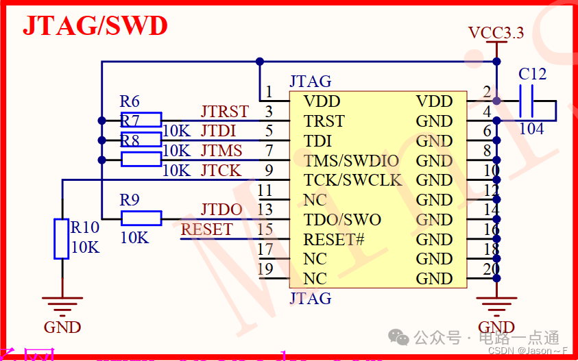
2. JTAG/SWD Debug Interface Circuit
The JTAG/SWD debug interface circuit adopts the standard JTAG connection, which is compatible with the SWD interface because SWD only requires four wires (SWCLK, SWDIO, VCC, and GND). It is important to note that this interface circuit provides 3.3V power to JLINK or ST-Link, so JLINK or ST-Link cannot power the STM32 core board; instead, the STM32 core board powers JLINK or ST-Link. JLINK and ST-Link can not only download programs but also perform online debugging of STM32 microcontrollers.
3. Clock Circuit
The MCU is an integrated chip composed of very complex digital circuits and other circuits, requiring a stable clock pulse signal to ensure normal operation. The clock is like the heart of the human body; it is the “power” source of the chip. Each time the clock generates a pulse, it pushes the processor to execute an instruction. In addition to the CPU, all peripherals on the chip (GPIO, I2C, SPI, etc.) require a clock, which highlights the importance of the clock. The higher the clock frequency at which the chip operates, the faster the chip processes, but the power consumption also increases. To balance power consumption and performance, microprocessors generally have multiple clock sources and also divide the clock into multiple sizes to adapt to the needs of different peripherals. Below is the clock tree of STM32. 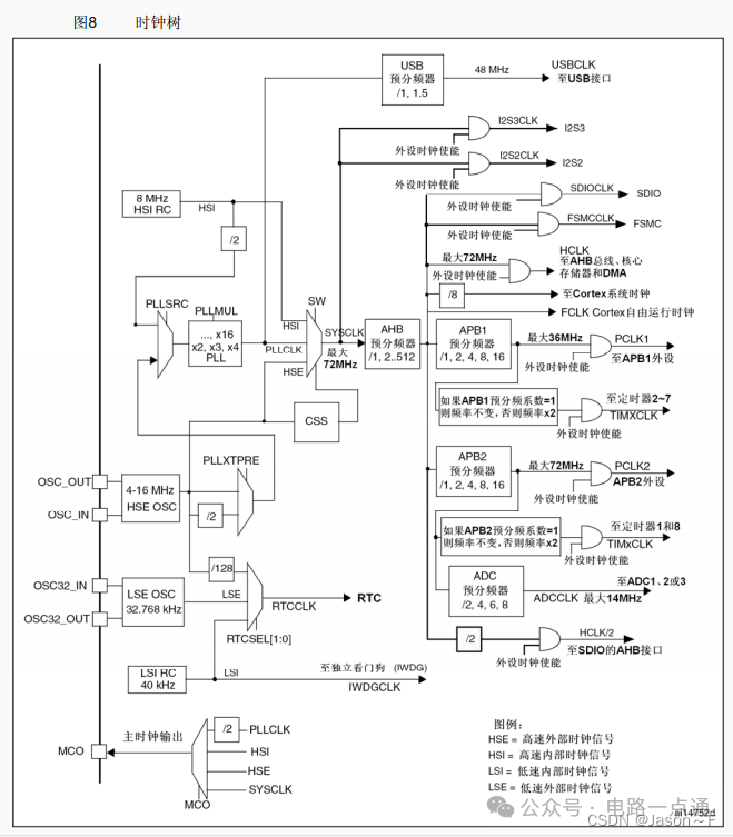
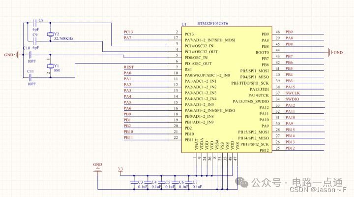 Here we will connect the two crystal oscillator circuits, power supply, and the network symbols of each pin accordingly. Except for the crystal oscillator and power supply, the remaining labels are connected to the pin headers we have drawn out. The crystal oscillator circuit includes an 8MHz main crystal oscillator and a 32.768kHz internal RTC real-time clock crystal oscillator. The clock crystal oscillator here is reserved; if anyone needs to use the clock, they can directly solder it on for convenience. The capacitors in parallel behind each crystal oscillator are the startup capacitors to facilitate the oscillation of the crystal oscillator, and the capacitors C3-C7 in the power supply part form a low-pass filter circuit to ensure better operation of the 32.
4. Reset Circuit
In embedded systems, due to external environmental interference, it is inevitable that programs may run away or crash, at which point a reset is needed to restart the MCU. This circuit connects a button to the NRST pin; once the button is pressed, NRST will be grounded, pulling down NRST to achieve a reset. 
Original link:https://blog.csdn.net/qq_59134387/article/details/127071871
— END —
Join the Fan Group
(Advertisements and peers are not allowed to enter)