“ The DAC of STM32F4xx is a 12-bit digital-to-analog module that supports dual-channel independent or synchronized output, capable of generating waveforms such as noise and triangle waves, and is compatible with various triggering methods and DMA transfers. It is widely used in audio, waveform generation, and other scenarios. This article introduces its configuration and applications to help grasp the key points of development.“
01
—
Introduction to STM32 DAC
The DAC in the STM32F4xx series is a 12-bit digital input, voltage output digital-to-analog converter. It can be configured in 8-bit or 12-bit mode, and in 12-bit mode, the data can be set to left-aligned or right-aligned, and can be used with the DMA controller for efficient data transfer.
Number of Channels
The vast majority of STM32F4 devices provide 2 independent DAC channels (for devices with fewer than 64 pins, only one channel may be available or no DAC may be present). Each channel has corresponding pins, such as DAC_OUT1 (PA4) and DAC_OUT2 (PA5), allowing for two independent or synchronized analog signal outputs.
Electrical Characteristics
Output Voltage Range: The output voltage range is from 0 to VREF+, where VREF+ is the reference voltage that can be obtained through an input reference voltage pin. The formula is DACoutput = VREF * DOR / 4095, where DOR is the value of the data output register.
Output Buffer: It integrates two output buffers, which can be enabled or disabled through the corresponding BOFFx bits in the DAC_CR register, to reduce output impedance, allowing it to drive external loads directly without the need for additional operational amplifiers.
Conversion Speed: Taking the STM32F407ZGT6 as an example, the typical conversion time is 3us, with a maximum of 6us, and the conversion speed can reach up to approximately 333K (limited by the output buffer RC load).
Linearity: In 12-bit mode, the linearity is very good, with maximum deviation usually within the specified range, ensuring the quality of the output signal and reducing signal distortion.
Application Scenarios
Audio Signal Processing: It can convert digital audio signals into analog audio signals to drive speakers, such as the STM32F4xx Black Pill combined with the PCM5102A USB DAC project, which can enhance headphone output quality and provide users with a better audio experience.
Waveform Generation: It supports triangle wave generation mode and noise generation mode, which can be used to generate specific waveforms, such as in signal generators, where the DAC can output continuous triangle waves or analog signals with random noise through configuration.
Motor Speed Control: It can convert the digital control signals output by the microcontroller into analog voltage signals to control the speed of the motor. The accuracy and stability of the DAC are crucial for the accuracy and stability of motor control.
Sensor Signal Simulation: In some data acquisition systems, the data collected by the ADC can be output through the DAC to simulate sensor signals, facilitating system debugging or simulating specific sensor input scenarios.

02
—
DAC Block Diagram
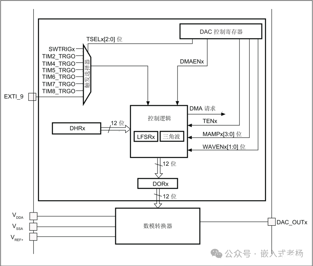
1.External Trigger Source Selection Module
Input Signals: Including software trigger signalsSWTRIGx, as well as timer trigger signalsTIM2_TRGO,TIM4_TRGO,TIM5_TRGO,TIM6_TRGO,TIM7_TRGO,TIM8_TRGO, and external interrupt signalsEXTI_9.
Selector: The trigger source is selected through the TSELx[2:0] bits. The function of this module is to determine the source of the DAC conversion start signal, which can be selected based on actual needs for software trigger, timer trigger, or external interrupt trigger.
2.Data Holding Register (DHRx)
Used to store the digital data to be converted, with a data width of 12 bits. It receives digital signals written from the microcontroller as the raw data for the digital-to-analog conversion.
3.Control Logic Module
Internal Structure: Includes a linear feedback shift registerLFSRx and a triangle wave generation module. LFSRx can be used to generate specific digital sequences, while the triangle wave generation module is used to generate triangle wave signals.
Control Signal Input: Receives signals from the DAC control register such as DMAENx (DMA enable signal), TENx (trigger enable signal), MAMPx[3:0] (analog output buffer amplifier waveform amplitude/mask setting signal), and WAVEx[1:0] (waveform generation enable and mode setting signal). These signals are used to control the operating mode of the DAC, such as whether to use DMA for data transfer, whether to enable trigger functions, set the gain of the analog output, and select the waveform mode to be generated (e.g., triangle wave, etc.).
Data Output: Outputs the processed 12-bit digital signal to the data output registerDORx.
4.Data Output Register (DORx)
Stores the 12-bit digital signal received from the control logic module, which is directly transmitted to the digital-to-analog converter for conversion.
5.Digital-to-Analog Converter
Is the core module of the DAC, which converts the 12-bit digital signal in DORx into an analog signal, outputting from the DAC_OUTx pins. The voltage range of the analog signal depends on the reference voltage VREF+ and the conversion characteristics of the digital-to-analog converter.
6.Power Supply and Reference Voltage Interface
V_DDA provides the analog power supply for the DAC, V_SSA is the analog ground, and V_REF+ is the reference voltage input pin. The reference voltage determines the upper limit of the voltage range of the analog signal output by the DAC. For example, when V_REF+ is connected to 3.3V, the theoretical analog voltage range output by the DAC is 0 – 3.3V.
7.DAC Control Register
Is used to configure various parameters of the DAC, such as the aforementioned DMAENx, TENx, MAMPx[3:0], and WAVEx[1:0] signals, which are set by this register to control the operating mode and performance of the DAC.
03
—
DAC Principles
The CPU or DMA first writes the 12-bit digital quantity into the data holding register DHRx; if the trigger is off (TENx=0), the data automatically enters the data output register DORx within one APB1 cycle. If the trigger is on (TENx=1), it will be loaded into DORx after 3 APB1 cycles when the selected trigger source (timer TRGO, EXTI, or software SWTRIG) arrives; then the 12-bit R-2R network (resistor ladder digital-to-analog conversion circuit) converts DORx into an analog voltage VOUT = VREF+ × DOR/4095 and outputs it to the DAC_OUTx pin. To achieve continuous waveforms, simply generate a fixed frequency trigger with a timer, and the DMA can automatically transfer the waveform table into DHRx in sync, allowing the DAC to “run itself” without CPU intervention.
1.Data Writing and Triggering
First, the microcontroller writes the 12-bit digital data to be converted into the data holding register DHRx. If TENx=0 (trigger off), the data automatically enters DORx within one APB1 cycle after being written to DHRx. If TENx=1 (trigger on), it must wait for the trigger event, and DORx will only be updated after 3 APB1 cycles.
Then, based on the settings of TSELx[2:0] bits, the trigger source is selected. If software trigger is selected, the DAC conversion is triggered when the corresponding software trigger bit (SWTRIGx) is set. If timer trigger is selected, the conversion is initiated when the corresponding timer (such as TIM2, TIM4, etc.) generates a trigger signal (TRGO). When external interrupt trigger is selected, the conversion is triggered when the EXTI_9 interrupt signal arrives.
2.Control Logic Processing
When the trigger signal arrives, the control logic module processes accordingly based on control signals such as DMAENx, TENx, MAMPx[3:0], and WAVENx[1:0].
If DMA is enabled (DMAENx is set), data to be converted can be automatically fetched from memory via DMA, improving data transfer efficiency.
According to the waveform mode set by WAVENx[1:0], the control logic module can generate specific waveforms such as triangle waves. For example, when set to generate triangle wave mode, the triangle wave generation module works, combined with DHRx and MAMPx[3:0] settings, the triangle wave generator is based on the initial value of DHRx, oscillating up and down, with the amplitude set by MAMPx[3:0], not exceeding ±(MAMPx+1) LSB.
3.DAC Data Format
• Resolution: 12 bits (can be trimmed to 8 bits).
• Alignment and Register Correspondence:
12-bit right-aligned: Write to DAC_DHR12Rx[11:0];
12-bit left-aligned: Write to DAC_DHR12Lx[15:4];
8-bit right-aligned: Write to DAC_DHR8Rx[7:0] (actually stored in internal DHRx[11:4]);
• The dual-channel synchronous mode also has dedicated “D” suffixed registers (DAC_DHR12RD, etc.), allowing 32-bit loading of CH1/CH2 simultaneously.
4.DAC Conversion Principles• Users can only write to DHRx, not directly to DORx.• No trigger (TENx=0): Data automatically transfers from DHRx → DORx → 12-bit R-2R network → analog output after 1 APB1 cycle.• With trigger (TENx=1): Must wait for the rising edge of the selected trigger source, loading DHRx→DORx after 3 APB1 cycles; then the output voltage stabilizes after tSETTLING (typically 3~4 µs).
5.DAC Output Voltage Calculation
The output voltage VOUT of the DAC is related to the reference voltage VREF+ and the input digital quantity N, calculated as follows:
For 12-bit DAC:VOUT = N/4095 × VREF+, where N is the input 12-bit digital quantity (range 0 – 4095). For example, when VREF+ is 3.3V and the input digital quantity N is 2048, VOUT = 2048/4095 × 3.3V ≈ 1.65V.
For 8-bit DAC:VOUT = N/255 × VREF+, where N is the input 8-bit digital quantity (range 0 – 255).
6.DAC Trigger Selection
The DAC trigger sources of STM32F4xx have various options, configured through the TSELx [2:0] bits in the control register:
Software Trigger: Configure TSELx [2:0] to a specific value to enable software trigger (SWTRIGx). When the relevant bits are set through software, the DAC conversion can be initiated. This method is suitable for scenarios where manual control of the conversion timing is required, such as performing digital-to-analog conversion at specific points in a program flow.
Timer Trigger: You can select the trigger signals from TIM2_TRGO, TIM4_TRGO, TIM5_TRGO, TIM6_TRGO, TIM7_TRGO, TIM8_TRGO, etc. In applications where periodic DAC conversion is needed, such as generating periodic analog waveforms (e.g., sine waves, triangle waves, etc.), a timer can generate fixed frequency trigger signals to precisely control the DAC conversion frequency.
External Interrupt Trigger: Use external interrupt signals such as EXTI_9 as the trigger source. When an external event occurs and generates the corresponding interrupt signal, it triggers the DAC conversion, suitable for digital-to-analog conversion scenarios driven by external events, such as control signals from external devices triggering the DAC to output specific voltages.
04
—
DAC Functions
The DAC (Digital-to-Analog Converter) of STM32F4xx has functions such as noise generation, triangle wave generation, independent triggering, and synchronized triggering. Below is an introduction to these functions and their principles:
DMA Request
When DAC_CR.DMAENx=1 and triggered by external sources such as timers or EXTI, DMA automatically transfers data from memory to DAC_DHRx→DAC_DORx, completing an analog output. In dual-channel mode, only one DMAENx can be enabled, allowing one DMA stream to drive two DACs simultaneously. Since there is no buffer queue, if DMA cannot respond to a new trigger in time (a new trigger occurs, but the previous DMA has not finished transferring data, causing the DAC to miss the new value), it will set the DMAUDRx underflow flag and stop the transfer, requiring software to clear the flag and reconfigure DMA/DAC to continue. Its function is to output any waveform continuously with precise timing without CPU intervention, significantly reducing CPU load while ensuring output reliability through the underflow interrupt mechanism.
Noise Generation Function
The DAC can generate pseudo-random noise (LFSR): The internal 12-bit linear feedback shift register updates once after each trigger event, its value is masked by MAMPx[3:0] and added to the DHRx base value, then output to DAC_OUTx.
Triangle Wave Generation Function
The DAC can output a symmetric triangle wave: Based on the DHRx base value, the internal counter increments/decrements ±1 with each trigger, with the amplitude set by MAMPx[3:0], peak-to-peak value = (MAMPx+1) LSB. Typical applications include motor ramp settings, linear frequency sweeping, low-cost function generators, etc.
Independent Trigger Function
Each DAC channel (CH1-PA4, CH2-PA5) has independent trigger units (TENx, TSELx, DMAENx, etc.), allowing CH1 and CH2 to use different trigger sources, different waveform parameters, and different update timings, completely independent of each other, suitable for “multi-channel, multi-rate” output scenarios.
Synchronized Trigger Function
By writing 32-bit data to the dual-channel data register DHRxxD (DHR12RD, DHR12LD, etc.) at once, CH1 and CH2 can be loaded simultaneously; then configuring the same trigger source (any TIMx_TRGO, EXTI9, or software trigger) allows both channels to copy DHRx to DORx at the same APB1 clock edge, achieving zero-phase difference synchronized output, commonly used in stereo audio, synchronized motor drives, etc.
Dual-Channel DAC Functionality
Through the two DAC channels and these three dual registers, 11 conversion function modes can be achieved.
|
Mode Number |
Mode Name |
Core Configuration and Principles |
|
1 |
Independent Trigger (No Waveform) |
Both channels trigger enabled (TEN1=TEN2=1), different trigger sources (TSEL1≠TSEL2), no waveform generation (WAVEx=00), data loaded through dual registers (e.g., DHR12RD), updating DORx upon individual triggers. |
|
2 |
Independent Trigger (Single LFSR) |
Different trigger sources (TSEL1≠TSEL2), both channels enable LFSR waveform (WAVEx=01), MAMPx same, LFSR value added to DHRx base value upon triggering to update DORx. |
|
3 |
Independent Trigger (Different LFSR) |
Different trigger sources, LFSR waveform enabled (WAVEx=01), different MAMPx, independent LFSR amplitudes for both channels, updating upon triggering. |
|
4 |
Independent Trigger (Single Triangle Wave) |
Different trigger sources, triangle wave enabled (WAVEx=1x), same MAMPx, triangle wave counter value added to DHRx base value upon triggering to update DORx. |
|
5 |
Independent Trigger (Different Triangle Waves) |
Different trigger sources, triangle wave enabled, different MAMPx, independent triangle wave amplitudes for both channels, updating upon triggering. |
|
6 |
Synchronized Software Start (No Trigger) |
No trigger enabled (TEN1=TEN2=0), dual-channel data loaded at once through dual registers, updating DORx simultaneously after 1 APB1 cycle, without external trigger. |
|
7 |
Synchronized Trigger (No Waveform) |
Same trigger sources (TSEL1=TSEL2), trigger enabled, no waveform generation, both channels update DHRx data to DORx simultaneously upon triggering. |
|
8 |
Synchronized Trigger (Single LFSR) |
Same trigger sources, LFSR waveform enabled, same MAMPx, both channels update LFSR values added to DHRx base value synchronously upon triggering. |
|
9 |
Synchronized Trigger (Different LFSR) |
Same trigger sources, LFSR waveform enabled, different MAMPx, both channels independently calculate and update synchronously upon triggering. |
|
10 |
Synchronized Trigger (Single Triangle Wave) |
Same trigger sources, triangle wave enabled, same MAMPx, both channels update triangle wave counter values added to DHRx base value synchronously upon triggering. |
|
11 |
Synchronized Trigger (Different Triangle Waves) |
Same trigger sources, triangle wave enabled, different MAMPx, both channels independently calculate and update synchronously upon triggering. |
05
—
Hardware Description
DAC_OUT1 (PA4) and DAC_OUT2 (PA5) are brought out from the development board, measured using an oscilloscope, with the oscilloscope probe’s ground connected to the analog ground (AGND) of the DAC circuit on the development board.
06
—
Program Design Example
Below is the code for implementing 11 conversion function modes for the dual-channel DAC (without using DMA).
If only one DAC channel (e.g., channel 1) is needed, modify as follows: delete the function declarations for the unused channel in dac_modes.h; in the mode functions of dac_modes.c, remove the configuration code for the unused channel (e.g., channel 2) (including HAL_DAC_ConfigChannel, HAL_DAC_SetValue, etc.), keeping only the configuration, start, and data settings for the target channel (e.g., channel 1); in main.c, delete the timer initialization for the unused channel (e.g., TIM4), and comment out the call to initialize that timer in the main function, while ensuring the trigger source timer for the target channel (e.g., TIM2) is initialized normally; for further simplification, remove the definitions related to the unused DAC channel from the global handle and the corresponding GPIO configuration.
dac_modes.h
#ifndef __DAC_MODES_H#define __DAC_MODES_H#include "stm32f4xx_hal.h"// Declare 11 mode functionsvoid DAC_Mode1_Independent_Trigger_NoWave(void);void DAC_Mode2_Independent_Trigger_SingleLFSR(void);void DAC_Mode3_Independent_Trigger_DiffLFSR(void);void DAC_Mode4_Independent_Trigger_SingleTriangle(void);void DAC_Mode5_Independent_Trigger_DiffTriangle(void);void DAC_Mode6_Sync_SoftStart(void);void DAC_Mode7_Sync_Trigger_NoWave(void);void DAC_Mode8_Sync_Trigger_SingleLFSR(void);void DAC_Mode9_Sync_Trigger_DiffLFSR(void);void DAC_Mode10_Sync_Trigger_SingleTriangle(void);void DAC_Mode11_Sync_Trigger_DiffTriangle(void);#endifdac_modes.c
#include "dac_modes.h"#include "stm32f4xx_hal.h"// External declarations: DAC and timer handles (must be defined in the initialization function)extern DAC_HandleTypeDef hdac;extern TIM_HandleTypeDef htim2; // Trigger source 1: for independent triggering of channel 1extern TIM_HandleTypeDef htim4; // Trigger source 2: for independent triggering of channel 2extern TIM_HandleTypeDef htim6; // Trigger source 3: for synchronized triggering// Channel base values (12-bit DAC range: 0~4095)static const uint32_t ch1_val = 2048; // Channel 1 base value (corresponding to midpoint voltage)static const uint32_t ch2_val = 3000; // Channel 2 base value/** * @brief Common auxiliary function: Quickly configure DAC channel parameters * @param hdac: DAC handle * @param cfg: Channel configuration structure * @param trigger: Trigger source (e.g., DAC_TRIGGER_T2_TRGO) * @param wave: Waveform mode (DAC_WAVE_NONE/LFSR/TRIANGLE) * @param amp: Amplitude parameter (LFSR mask or triangle wave amplitude) */static void DAC_ConfigChannel(DAC_HandleTypeDef *hdac, DAC_ChannelConfTypeDef *cfg, uint32_t trigger, uint32_t wave, uint32_t amp){ cfg->DAC_Trigger = trigger; // Trigger source selection cfg->DAC_WaveGeneration = wave; // Waveform generation mode cfg->DAC_LFSRUnmask_TriangleAmplitude = amp; // Amplitude parameter cfg->DAC_OutputBuffer = DAC_OUTPUTBUFFER_ENABLE; // Enable output buffer (reduce output impedance)}/* * @brief Mode 1: Independent Trigger (No Waveform) * @note Channel 1 uses TIM2 trigger, channel 2 uses TIM4 trigger (independent sources), no waveform generation */void DAC_Mode1_Independent_Trigger_NoWave(void){ DAC_ChannelConfTypeDef cfg = {0}; // Configure channel 1: TIM2 trigger, no waveform DAC_ConfigChannel(&hdac, &cfg, DAC_TRIGGER_T2_TRGO, DAC_WAVE_NONE, 0); HAL_DAC_ConfigChannel(&hdac, &cfg, DAC_CHANNEL_1); // Configure channel 2: TIM4 trigger (independent from channel 1), no waveform cfg.DAC_Trigger = DAC_TRIGGER_T3_TRGO; // Independent trigger source HAL_DAC_ConfigChannel(&hdac, &cfg, DAC_CHANNEL_2); // Set channel output values HAL_DAC_SetValue(&hdac, DAC_CHANNEL_1, DAC_ALIGN_12B_R, ch1_val); HAL_DAC_SetValue(&hdac, DAC_CHANNEL_2, DAC_ALIGN_12B_R, ch2_val); // Start timers and DAC HAL_TIM_Base_Start(&htim2); // Start TIM2 (trigger source) HAL_TIM_Base_Start(&htim4); // Start TIM4 (trigger source) HAL_DAC_Start(&hdac, DAC_CHANNEL_1); // Start channel 1 HAL_DAC_Start(&hdac, DAC_CHANNEL_2); // Start channel 2}/* * @brief Mode 2: Independent Trigger (Single LFSR) * @note Channel 1 uses TIM2 trigger, channel 2 uses TIM4 trigger (independent sources), both generate LFSR noise (same amplitude) */void DAC_Mode2_Independent_Trigger_SingleLFSR(void){ DAC_ChannelConfTypeDef cfg = {0}; // Configure channel 1: TIM2 trigger, LFSR noise (amplitude: full range of 12 bits) DAC_ConfigChannel(&hdac, &cfg, DAC_TRIGGER_T2_TRGO, DAC_WAVE_LFSR, DAC_LFSRUNMASK_BITS11_0); HAL_DAC_ConfigChannel(&hdac, &cfg, DAC_CHANNEL_1); // Configure channel 2: TIM4 trigger (independent source), same amplitude LFSR noise cfg.DAC_Trigger = DAC_TRIGGER_T3_TRGO; HAL_DAC_ConfigChannel(&hdac, &cfg, DAC_CHANNEL_2); // Set base values (noise added to base value) HAL_DAC_SetValue(&hdac, DAC_CHANNEL_1, DAC_ALIGN_12B_R, ch1_val); HAL_DAC_SetValue(&hdac, DAC_CHANNEL_2, DAC_ALIGN_12B_R, ch2_val); // Start timers and DAC HAL_TIM_Base_Start(&htim2); HAL_TIM_Base_Start(&htim4); HAL_DAC_Start(&hdac, DAC_CHANNEL_1); HAL_DAC_Start(&hdac, DAC_CHANNEL_2);}/* * @brief Mode 3: Independent Trigger (Different LFSR) * @note Channel 1 uses TIM2 trigger, channel 2 uses TIM4 trigger, LFSR noise amplitudes differ */void DAC_Mode3_Independent_Trigger_DiffLFSR(void){ DAC_ChannelConfTypeDef cfg = {0}; // Channel 1: TIM2 trigger, LFSR noise (amplitude: low 7 bits) DAC_ConfigChannel(&hdac, &cfg, DAC_TRIGGER_T2_TRGO, DAC_WAVE_LFSR, DAC_LFSRUNMASK_BITS6_0); HAL_DAC_ConfigChannel(&hdac, &cfg, DAC_CHANNEL_1); // Channel 2: TIM4 trigger, LFSR noise (amplitude: full range of 12 bits) cfg.DAC_Trigger = DAC_TRIGGER_T3_TRGO; cfg.DAC_LFSRUnmask_TriangleAmplitude = DAC_LFSRUNMASK_BITS11_0; HAL_DAC_ConfigChannel(&hdac, &cfg, DAC_CHANNEL_2); // Set base values HAL_DAC_SetValue(&hdac, DAC_CHANNEL_1, DAC_ALIGN_12B_R, ch1_val); HAL_DAC_SetValue(&hdac, DAC_CHANNEL_2, DAC_ALIGN_12B_R, ch2_val); // Start timers and DAC HAL_TIM_Base_Start(&htim2); HAL_TIM_Base_Start(&htim4); HAL_DAC_Start(&hdac, DAC_CHANNEL_1); HAL_DAC_Start(&hdac, DAC_CHANNEL_2);}/* * @brief Mode 4: Independent Trigger (Single Triangle Wave) * @note Channel 1 uses TIM2 trigger, channel 2 uses TIM4 trigger, triangle wave amplitudes are the same */void DAC_Mode4_Independent_Trigger_SingleTriangle(void){ DAC_ChannelConfTypeDef cfg = {0}; // Channel 1: TIM2 trigger, triangle wave (amplitude: 511 LSB) DAC_ConfigChannel(&hdac, &cfg, DAC_TRIGGER_T2_TRGO, DAC_WAVE_TRIANGLE, DAC_TRIANGLEAMPLITUDE_511); HAL_DAC_ConfigChannel(&hdac, &cfg, DAC_CHANNEL_1); // Channel 2: TIM4 trigger, same amplitude triangle wave cfg.DAC_Trigger = DAC_TRIGGER_T3_TRGO; HAL_DAC_ConfigChannel(&hdac, &cfg, DAC_CHANNEL_2); // Set base values (triangle wave added to base value) HAL_DAC_SetValue(&hdac, DAC_CHANNEL_1, DAC_ALIGN_12B_R, ch1_val); HAL_DAC_SetValue(&hdac, DAC_CHANNEL_2, DAC_ALIGN_12B_R, ch2_val); // Start timers and DAC HAL_TIM_Base_Start(&htim2); HAL_TIM_Base_Start(&htim4); HAL_DAC_Start(&hdac, DAC_CHANNEL_1); HAL_DAC_Start(&hdac, DAC_CHANNEL_2);}/* * @brief Mode 5: Independent Trigger (Different Triangle Waves) * @note Channel 1 uses TIM2 trigger, channel 2 uses TIM4 trigger, triangle wave amplitudes differ */void DAC_Mode5_Independent_Trigger_DiffTriangle(void){ DAC_ChannelConfTypeDef cfg = {0}; // Channel 1: TIM2 trigger, triangle wave (amplitude: 255 LSB) DAC_ConfigChannel(&hdac, &cfg, DAC_TRIGGER_T2_TRGO, DAC_WAVE_TRIANGLE, DAC_TRIANGLEAMPLITUDE_255); HAL_DAC_ConfigChannel(&hdac, &cfg, DAC_CHANNEL_1); // Channel 2: TIM4 trigger, triangle wave (amplitude: 1023 LSB) cfg.DAC_Trigger = DAC_TRIGGER_T3_TRGO; cfg.DAC_LFSRUnmask_TriangleAmplitude = DAC_TRIANGLEAMPLITUDE_1023; HAL_DAC_ConfigChannel(&hdac, &cfg, DAC_CHANNEL_2); // Set base values HAL_DAC_SetValue(&hdac, DAC_CHANNEL_1, DAC_ALIGN_12B_R, ch1_val); HAL_DAC_SetValue(&hdac, DAC_CHANNEL_2, DAC_ALIGN_12B_R, ch2_val); // Start timers and DAC HAL_TIM_Base_Start(&htim2); HAL_TIM_Base_Start(&htim4); HAL_DAC_Start(&hdac, DAC_CHANNEL_1); HAL_DAC_Start(&hdac, DAC_CHANNEL_2);}/* * @brief Mode 6: Synchronized Software Start (No Trigger) * @note No external trigger, dual-channel data written at once through software, synchronized output */void DAC_Mode6_Sync_SoftStart(void){ DAC_ChannelConfTypeDef cfg = {0}; // Configure dual channels: no trigger source, no waveform DAC_ConfigChannel(&hdac, &cfg, DAC_TRIGGER_NONE, DAC_WAVE_NONE, 0); HAL_DAC_ConfigChannel(&hdac, &cfg, DAC_CHANNEL_1); HAL_DAC_ConfigChannel(&hdac, &cfg, DAC_CHANNEL_2); // Start DAC and write dual-channel data (effective synchronously after 1 APB1 cycle) HAL_DAC_Start(&hdac, DAC_CHANNEL_1); HAL_DAC_Start(&hdac, DAC_CHANNEL_2); HAL_DAC_SetDualChannelData(&hdac, DAC_ALIGN_12B_R, ch1_val, ch2_val);}/* * @brief Mode 7: Synchronized Trigger (No Waveform) * @note Dual channels share TIM6 trigger source, synchronized output of base values */void DAC_Mode7_Sync_Trigger_NoWave(void){ DAC_ChannelConfTypeDef cfg = {0}; // Configure dual channels: TIM6 trigger (synchronized source), no waveform DAC_ConfigChannel(&hdac, &cfg, DAC_TRIGGER_T6_TRGO, DAC_WAVE_NONE, 0); HAL_DAC_ConfigChannel(&hdac, &cfg, DAC_CHANNEL_1); HAL_DAC_ConfigChannel(&hdac, &cfg, DAC_CHANNEL_2); // Start DAC and timer (synchronized output upon triggering) HAL_DAC_Start(&hdac, DAC_CHANNEL_1); HAL_DAC_Start(&hdac, DAC_CHANNEL_2); HAL_DACEx_DualSetValue(&hdac, DAC_ALIGN_12B_R, ch1_val, ch2_val); // Dual-channel data HAL_TIM_Base_Start(&htim6); // Start synchronized trigger source}/* * @brief Mode 8: Synchronized Trigger (Single LFSR) * @note Dual channels share TIM6 trigger source, synchronized output of same amplitude LFSR noise */void DAC_Mode8_Sync_Trigger_SingleLFSR(void){ DAC_ChannelConfTypeDef cfg = {0}; // Configure dual channels: TIM6 trigger, LFSR noise (same amplitude) DAC_ConfigChannel(&hdac, &cfg, DAC_TRIGGER_T6_TRGO, DAC_WAVE_LFSR, DAC_LFSRUNMASK_BITS11_0); HAL_DAC_ConfigChannel(&hdac, &cfg, DAC_CHANNEL_1); HAL_DAC_ConfigChannel(&hdac, &cfg, DAC_CHANNEL_2); // Start DAC and timer HAL_DAC_Start(&hdac, DAC_CHANNEL_1); HAL_DAC_Start(&hdac, DAC_CHANNEL_2); HAL_DACEx_DualSetValue(&hdac, DAC_ALIGN_12B_R, ch1_val, ch2_val); HAL_TIM_Base_Start(&htim6);}/* * @brief Mode 9: Synchronized Trigger (Different LFSR) * @note Dual channels share TIM6 trigger source, output different amplitude LFSR noise */void DAC_Mode9_Sync_Trigger_DiffLFSR(void){ DAC_ChannelConfTypeDef cfg = {0}; // Channel 1: TIM6 trigger, LFSR noise (amplitude: low 7 bits) DAC_ConfigChannel(&hdac, &cfg, DAC_TRIGGER_T6_TRGO, DAC_WAVE_LFSR, DAC_LFSRUNMASK_BITS6_0); HAL_DAC_ConfigChannel(&hdac, &cfg, DAC_CHANNEL_1); // Channel 2: same trigger source, LFSR noise (amplitude: full range of 12 bits) cfg.DAC_LFSRUnmask_TriangleAmplitude = DAC_LFSRUNMASK_BITS11_0; HAL_DAC_ConfigChannel(&hdac, &cfg, DAC_CHANNEL_2); // Start DAC and timer HAL_DAC_Start(&hdac, DAC_CHANNEL_1); HAL_DAC_Start(&hdac, DAC_CHANNEL_2); HAL_DACEx_DualSetValue(&hdac, DAC_ALIGN_12B_R, ch1_val, ch2_val); HAL_TIM_Base_Start(&htim6);}/* * @brief Mode 10: Synchronized Trigger (Single Triangle Wave) * @note Dual channels share TIM6 trigger source, synchronized output of same amplitude triangle wave */void DAC_Mode10_Sync_Trigger_SingleTriangle(void){ DAC_ChannelConfTypeDef cfg = {0}; // Configure dual channels: TIM6 trigger, triangle wave (same amplitude) DAC_ConfigChannel(&hdac, &cfg, DAC_TRIGGER_T6_TRGO, DAC_WAVE_TRIANGLE, DAC_TRIANGLEAMPLITUDE_511); HAL_DAC_ConfigChannel(&hdac, &cfg, DAC_CHANNEL_1); HAL_DAC_ConfigChannel(&hdac, &cfg, DAC_CHANNEL_2); // Start DAC and timer HAL_DAC_Start(&hdac, DAC_CHANNEL_1); HAL_DAC_Start(&hdac, DAC_CHANNEL_2); HAL_DACEx_DualSetValue(&hdac, DAC_ALIGN_12B_R, ch1_val, ch2_val); HAL_TIM_Base_Start(&htim6);}/* * @brief Mode 11: Synchronized Trigger (Different Triangle Waves) * @note Dual channels share TIM6 trigger source, output different amplitude triangle waves */void DAC_Mode11_Sync_Trigger_DiffTriangle(void){ DAC_ChannelConfTypeDef cfg = {0}; // Channel 1: TIM6 trigger, triangle wave (amplitude: 255 LSB) DAC_ConfigChannel(&hdac, &cfg, DAC_TRIGGER_T6_TRGO, DAC_WAVE_TRIANGLE, DAC_TRIANGLEAMPLITUDE_255); HAL_DAC_ConfigChannel(&hdac, &cfg, DAC_CHANNEL_1); // Channel 2: same trigger source, triangle wave (amplitude: 1023 LSB) cfg.DAC_LFSRUnmask_TriangleAmplitude = DAC_TRIANGLEAMPLITUDE_1023; HAL_DAC_ConfigChannel(&hdac, &cfg, DAC_CHANNEL_2); // Start DAC and timer HAL_DAC_Start(&hdac, DAC_CHANNEL_1); HAL_DAC_Start(&hdac, DAC_CHANNEL_2); HAL_DACEx_DualSetValue(&hdac, DAC_ALIGN_12B_R, ch1_val, ch2_val);}/** * @brief main.c */int main(void){ HAL_Init(); SystemClock_Config(); // Configure system clock to 168MHz MX_GPIO_Init(); MX_DAC_Init(); MX_TIM2_Init(); MX_TIM4_Init(); MX_TIM6_Init(); // Select test mode (1~11) DAC_Mode1_Independent_Trigger_NoWave(); while (1) { HAL_Delay(1000); // Main loop idle }}/* * @brief System Clock Configuration (168MHz) */void SystemClock_Config(void){ RCC_OscInitTypeDef RCC_OscInitStruct = {0}; RCC_ClkInitTypeDef RCC_ClkInitStruct = {0}; RCC_OscInitStruct.OscillatorType = RCC_OSCILLATORTYPE_HSE; RCC_OscInitStruct.HSEState = RCC_HSE_ON; RCC_OscInitStruct.PLL.PLLState = RCC_PLL_ON; RCC_OscInitStruct.PLL.PLLSource = RCC_PLLSOURCE_HSE; RCC_OscInitStruct.PLL.PLLM = 25; RCC_OscInitStruct.PLL.PLLN = 336; RCC_OscInitStruct.PLL.PLLP = RCC_PLLP_DIV2; // 168MHz RCC_OscInitStruct.PLL.PLLQ = 4; HAL_RCC_OscConfig(&RCC_OscInitStruct); RCC_ClkInitStruct.ClockType = RCC_CLOCKTYPE_HCLK|RCC_CLOCKTYPE_SYSCLK |RCC_CLOCKTYPE_PCLK1|RCC_CLOCKTYPE_PCLK2; RCC_ClkInitStruct.SYSCLKSource = RCC_SYSCLKSOURCE_PLLCLK; RCC_ClkInitStruct.AHBCLKDivider = RCC_SYSCLK_DIV1; RCC_ClkInitStruct.APB1CLKDivider = RCC_HCLK_DIV4; // 42MHz RCC_ClkInitStruct.APB2CLKDivider = RCC_HCLK_DIV2; // 84MHz HAL_RCC_ClkConfig(&RCC_ClkInitStruct, FLASH_LATENCY_5);}/* * @brief Error Handler */void Error_Handler(void){ while(1); // Infinite loop waiting for reset}
This article’s case uses the following hardware and software:
1. Microcontroller model: STM32F407ZGT6 (25MHz external crystal);
2. Software development environment: Keil MDK v5.36;
3. Pack version: STM32F4xx_DFP v3.0.0;
4. Compiler: ARM Compiler v5;
5. STM32 project version: Standard HAL library or register version;
6. Downloader: JLINK downloader, SWD interface;
7. This software and hardware case is for personal learning only and not for commercial use.
References:
“STM32F4xx Reference Manual (RM0090)”;
“STM32F405xx STM32F407xx Datasheet (DS8626)”.