1. Introduction to SPI
SPI, which stands for Serial Peripheral Interface, is a synchronous serial communication protocol originally defined by Motorola for its MC68HCXX series processors. The SPI interface is primarily used for communication between EEPROMs, FLASH memory, real-time clocks, ADCs, as well as digital signal processors and digital signal decoders. SPI is a high-speed, full-duplex, synchronous communication bus that only requires four lines on the chip pins, saving pin space and providing convenience for PCB layout. Due to its simplicity and ease of use, an increasing number of chips are integrating this communication protocol.
2. Features of SPI
2.1 Master-Slave Control Mode
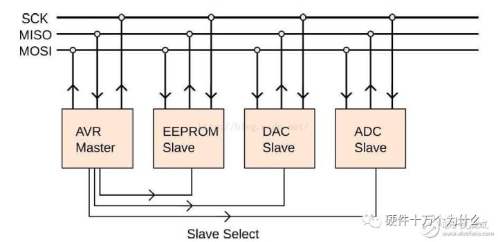
SPI specifies that communication between two SPI devices must be controlled by a master device. A master device can control multiple slave devices by providing a clock signal and selecting the slave device through Slave Select (SS). The SPI protocol also stipulates that the clock for the slave device is provided by the master device through the SCK pin; the slave device cannot generate or control the clock. Without a clock, the slave device cannot operate normally.
2.2 Synchronous Data Transmission
The master device generates corresponding clock pulses based on the data to be exchanged, forming a clock signal that controls when data is exchanged and when received data is sampled between the two SPI devices, ensuring that data is transmitted synchronously.
2.3 Data Exchanges
The data transfer between SPI devices is referred to as data exchange because the SPI protocol stipulates that an SPI device cannot act solely as a “transmitter” or “receiver” during data communication. In each clock cycle, SPI devices send and receive one bit of data, effectively exchanging one bit of data. A slave device must be accessed by the master device before it can receive control signals sent from the master. Therefore, the master device must first select the desired slave device using the SS/CS pin. During data transmission, each received data must be sampled before the next data transmission. If the previously received data is not read, it may be discarded, leading to the failure of the SPI physical module. Thus, it is common practice in programs to read the data from the SPI device after the SPI transmission, even if this data (Dummy Data) is not useful in our program.
2.4 Four Transmission Modes of SPI
There are four transmission modes based on rising edge, falling edge, leading edge, and trailing edge. Additionally, there are MSB and LSB transmission methods.
2.5 Only Master and Slave Modes
There is no distinction between read and write, as each SPI transaction involves data exchange between the master and slave devices. In other words, sending data will always result in receiving data; to receive data, one must first send data.
3. Working Mechanism
3.1 Overview
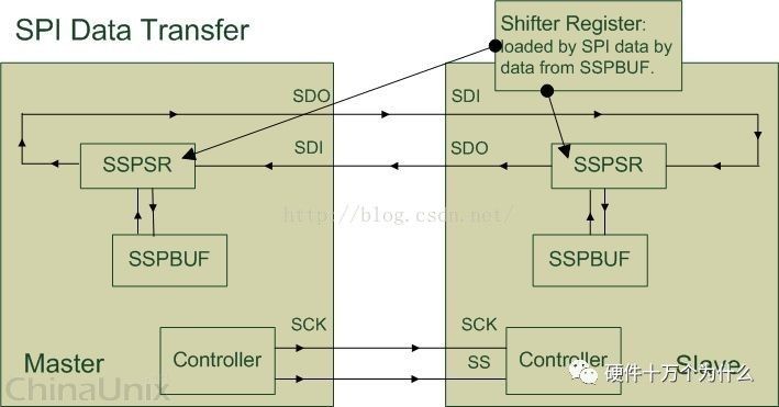
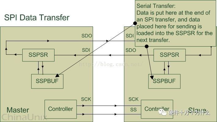
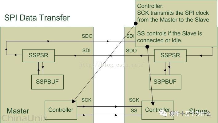
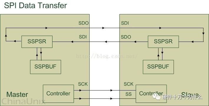 The above image provides a simple description of communication between SPI devices. Below, we will explain several components shown in the diagram: SSPBUF, Synchronous Serial Port Buffer, generally refers to the internal buffer of the SPI device, typically implemented as FIFO, which stores temporary data during transmission; SSPSR, Synchronous Serial Port Register, refers to the shift register within the SPI device, which shifts data in or out of SSPBUF based on the configured data bit-width; Controller, refers to the control register within the SPI device, which can be configured to set the transmission mode of the SPI bus. Typically, we only need to program the four pins described in the diagram to control data communication between SPI devices: SCK, Serial Clock, primarily used for the master device to transmit clock signals to the slave device, controlling the timing and rate of data exchange; SS/CS, Slave Select/Chip Select, used for the master device to select the slave device, allowing the selected slave device to be accessed by the master; SDO/MOSI, Serial Data Output/Master Out Slave In, also known as Tx-Channel on the master, serves as the data output for sending data from the SPI device; SDI/MISO, Serial Data Input/Master In Slave Out, also known as Rx-Channel on the master, serves as the data input for receiving data from the SPI device. During communication, a data loop is formed between the master and slave devices, as illustrated in the diagram, where data is shifted in and out of SSPBUF via SDO and SDI pins, with SSPSR controlling the data movement, and the controller determining the communication mode of the SPI bus, while SCK transmits the clock signal.
3.2 Timing
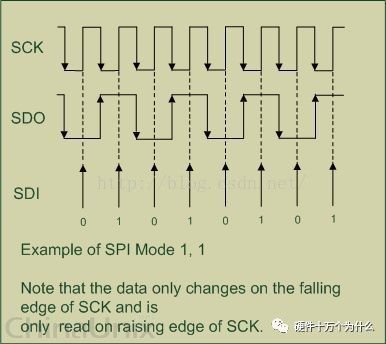 The above image illustrates the working mechanism of the SPI protocol through the exchange of 1 Byte of data between the master and slave devices. First, let’s explain the concepts of phase and polarity.
3.2.1 SPI Related Abbreviations
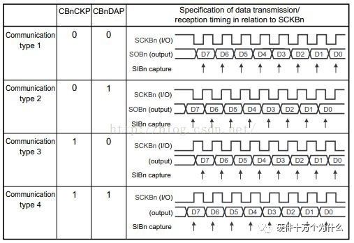
The polarity (CPOL) and phase (CPHA) of SPI are commonly denoted as follows: (1) CKPOL (Clock Polarity) = CPOL = POL = Polarity = (Clock) Polarity (2) CKPHA (Clock Phase) = CPHA = PHA = Phase = (Clock) Phase (3) SCK=SCLK=SPI Clock (4) Edge = the moment of clock level change, either rising edge or falling edge. Within one clock cycle, there are two edges, referred to as: Leading edge = the first edge, for a starting voltage of 1, it is when it changes from 1 to 0; for a starting voltage of 0, it is when it changes from 0 to 1; Trailing edge = the second edge, for a starting voltage of 1, it is when it changes from 0 to 1 (after the first 1 to 0 transition); for a starting voltage of 0, it is when it changes from 1 to 0.
3.2.2 SPI Phase and Polarity
CPOL and CPHA can each be 0 or 1, resulting in four combinations: Mode 0 CPOL=0, CPHA=0; Mode 1 CPOL=0, CPHA=1; Mode 2 CPOL=1, CPHA=0; Mode 3 CPOL=1, CPHA=1.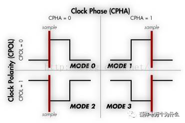
3.2.3 CPOL Polarity
First, let’s define the idle state of the SCLK clock, which is the state of SCLK before and after sending 8 bits of data. The active state of SCLK occurs when data is being sent. In brief, Clock Polarity = IDLE state of SCK. In detail: CPOL indicates whether the idle state of SCLK is low (0) or high (1): CPOL=0 means the clock is low when idle, so when SCLK is active, it is high (active-high); CPOL=1 means the clock is high when idle, so when SCLK is active, it is low (active-low).
3.2.4 CPHA Phase
To clarify, capture strobe = latch = read = sample, all refer to data sampling, the moment when data is valid. The phase corresponds to which edge (first or second) the data is sampled. 0 corresponds to the first edge, and 1 corresponds to the second edge. For CPHA=0, it indicates the first edge: for CPOL=0, the idle state is low, so the first edge is from low to high (rising edge); for CPOL=1, the idle state is high, so the first edge is from high to low (falling edge); for CPHA=1, it indicates the second edge: for CPOL=0, the idle state is low, so the second edge is from high to low (falling edge); for CPOL=1, the idle state is high, so the first edge is from low to high (rising edge); the above diagram makes it easier to understand.
3.2.5 How to Set SPI Polarity and Phase in Software
SPI consists of master and slave devices that communicate via the SPI protocol. The mode of the SPI slave device determines the mode of the master device. Therefore, it is essential to understand the mode of the slave device before configuring the master device to match the slave’s mode for proper communication. The slave device’s SPI mode can be:
3.2.5.1 Fixed, determined by the SPI slave hardware
The specific mode of the SPI slave device is described in the relevant datasheet, which must be consulted to find the description regarding whether the idle state is high or low, determining CPOL as 0 or 1; then, based on the established CPOL value, it can be inferred whether CPHA is 0 or 1 based on whether data is sampled on the rising or falling edge.
3.2.5.2 Configurable, set by software
The slave device is also an SPI controller that supports all four modes, allowing it to be set to any desired mode. Once the mode of the slave device is known, the master device’s SPI mode can be configured to match the slave’s mode for proper communication. Regarding how to configure CPOL and CPHA, it is generally done by writing to the corresponding bits in the SPI controller’s registers for CPOL and CPHA, setting them to 0 or 1.
3.3 SSPSR
 SSPSR is the internal shift register of the SPI device. Its primary function is to shift data in or out of SSPBUF based on the state of the SPI clock signal, with the size of the data shifted determined by Bus-Width and Channel-Width. Bus-Width specifies the unit of data transfer from the address bus to the master device. For example, if we want to write 16 Bytes of data to the SSPBUF of the master device, we first set the Bus-Width in the master’s configuration register to Byte; then we write data to the Tx-Data shift register at the address bus entry, shifting 1 Byte of data at a time (using the writeb function). After writing 1 Byte, the Tx-Data shift register of the master device automatically shifts the 1 Byte of data from the address bus into SSPBUF; this action needs to be repeated 16 times. Channel-Width specifies the unit of data transfer between the master and slave devices. Similar to Bus-Width, the internal shift register of the master device automatically shifts data from Master-SSPBUF to Slave-SDI via the Master-SDO pin, while Slave-SSPSR shifts each received data into Slave-SSPBUF. Typically, Bus-Width is always greater than or equal to Channel-Width, ensuring that data exchange frequency between the master and slave does not exceed the frequency of data exchange between the address bus and the master, preventing invalid data from being stored in SSPBUF.
3.4 SSPBUF
 We know that the data exchanged between the master and slave during each clock cycle is actually copied from the internal shift register of the SPI from SSPBUF. We can indirectly control the internal SSPBUF of the SPI device by reading and writing data to the corresponding registers (Tx-Data / Rx-Data register) of SSPBUF. For example, before sending data, we should first write the data to be sent into the Tx-Data register of the master; this data will be automatically shifted into Master-SSPBUF by the Master-SSPSR based on Bus-Width, and then this data will be shifted out from Master-SSPBUF according to Channel-Width through the Master-SDO pin to the Slave-SDI pin, while Slave-SSPSR shifts the received data from Slave-SDI into Slave-SSPBUF. Simultaneously, the data in Slave-SSPBUF is sent to Master-SDI via Slave-SDO, and Master-SSPSR shifts the received data from Master-SDI into Master-SSPBUF. After a single data transfer is completed, the user program can read the exchanged data from the Rx-Data register of the master device.
3.5 Controller
 The controller within the master device primarily controls the slave device through clock signals and slave select signals. The slave device will wait until it receives the slave select signal from the master, then operates based on the clock signal. The slave select operation of the master device must be implemented by the program. For example, the program pulls the SS/CS pin low to initiate data communication with the SPI device; when the program wants to end data communication, it pulls the SS/CS pin high.
4. Example of SPI
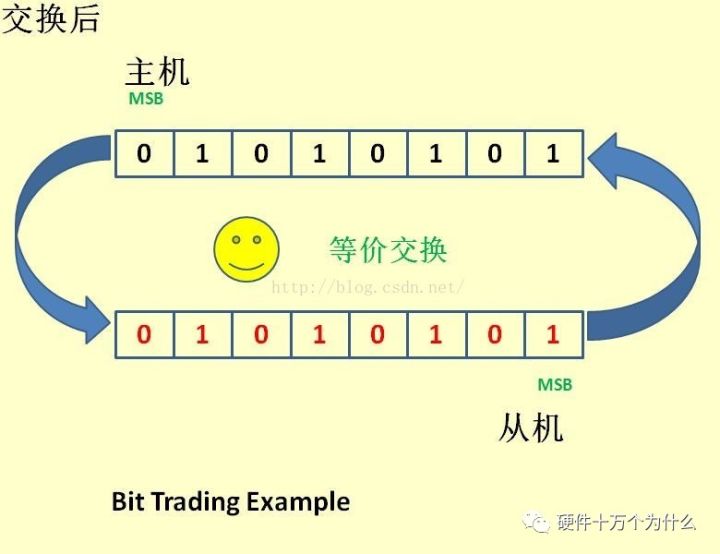
Having discussed so much, let me provide an example to help everyone understand. SPI is a ring bus structure composed of SS (CS), SCK, SDI, and SDO, and its timing is quite simple, primarily controlled by SCK, with two bidirectional shift registers exchanging data. Suppose the following 8-bit register contains the data to be sent, 10101010, with data sent on the rising edge and received on the falling edge, sending the high bit first. When the first rising edge arrives, the data will be SDO=1; the register will be 0101010x. When the falling edge arrives, the level on SDI will be stored in the register, so now the register will be 0101010sdi. After 8 clock pulses, the contents of the two registers will have exchanged once. This completes one SPI timing sequence. For example, suppose the master and slave are initialized and ready, with the master’s sbuff=0xaa and the slave’s sbuff=0x55. Below, I will demonstrate the data situation for the 8 clock cycles of SPI step by step: assuming data is sent on the rising edge.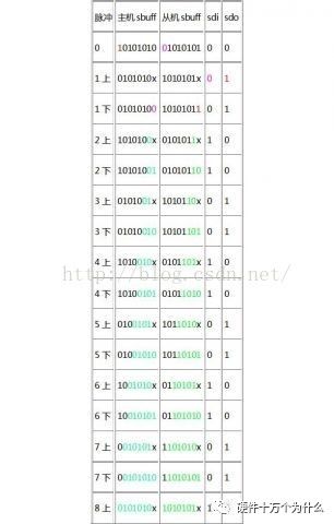 This completes the exchange of 8 bits between the two registers, with the upper part indicating the rising edge and the lower part indicating the falling edge, with SDI and SDO relative to the master. We are getting close to understanding; the next step is to convert the above process into an animation.
This article is reproduced from CSDN.