


Results Introduction
The research on two-dimensional (2D) transition metal dichalcogenide (TMD) layers has rapidly developed, focusing on revealing the changes in electrical and optical properties dependent on their morphology and/or chemical composition. Many 2D TMD layers have been found to exhibit these transitional characteristics (e.g., layer-number-dependent bandgap modulation), which are mostly observed in TMD layers using Group VI transition metals such as molybdenum (Mo) and tungsten (W). Recently, Group X elements (such as platinum (Pt) and palladium (Pd)) have gradually attracted attention as transition metals for 2D TMDs due to their unique advantages compared to traditional Group VI metals.Among them, palladium (Pd)-based TMDs, such as palladium diselenide (PdSe2), have more favorable properties compared to platinum (Pt)-based materials due to the simpler processing, lower cost, and better environmental stability of palladium.
The synthesis of 2D PdSe2 layers has been explored through various methods, among which chemical vapor deposition (CVD) is particularly promising due to its scalable process and assurance of high spatial uniformity. Professor Yeonwoong Jung’s team at the University of Central Florida achieved large-area growth of 2D PdSe2 layers at low temperatures below 330°C by directly selenizing Pd precursor films. Using their precisely controlled composition and morphology, we systematically introduced a strong transition from semiconductor to metal through two independent physical and chemical methods, namely thickness modulation and anion exchange (Se-to-Te).
Regarding the physical method, the thin 2D PdSe2 layers prepared from palladium films with a thickness of less than 3 nanometers exhibit significant semiconductor characteristics, accompanied by a hole mobility of 2.32 cm²/V·s, while thicker layers exhibit metallic characteristics regardless of thickness variations. Regarding the chemical method, the thin semiconductor 2D PdSe2 layers can be transformed into metallic PdTe2 layers through subsequent tellurization reactions at 330°C. The converted 2D PdTe2 layers show a bandgap reduction from 0.7 eV to 0 eV, accompanied by metallic characteristics that remain unchanged in thickness, which have been validated through various spectroscopic techniques. Utilizing these controlled transition characteristics, we can manufacture “fully 2D” flexible devices that employ semiconductor 2D layer channels and metallic 2D layer electrodes at the wafer scale.
Figure Introduction
 Figure 1. Thickness variation growth and characterization of 2D PdSe2 layers. (a) Schematic diagram of CVD growth of 2D PdSe2 layers. (b) Raman spectra of 2D PdSe2 layers prepared with five different palladium thicknesses. (c) Raman spectra obtained from different locations of the same sample with a palladium thickness of 2.1 nm. The inset shows the optical microscope image of the sample. (d) Atomic force microscopy height profile and representative atomic force microscopy morphology image (inset) of 2D PdSe2 layers prepared with five different palladium thicknesses. (e) Correlation between palladium thickness and the thickness of the generated 2D PdSe2 layer, along with a representative atomic force microscopy morphology image (inset). (f), (g): TEM characteristics of the 2D PdSe2 layers showing thickness variation through (f) HR-TEM and (g) SAED images.

Figure 2. Field-effect transistor measurements show the transition from semiconductor to metal in 2D PdSe2 layers with varying thickness. (a) Ids-Vds curves of the field-effect transistor using thin 2D PdSe2 layers (palladium thickness = 2.1 nm) as Vg varies. (b) Ids-Vg curve of the same field-effect transistor in (a) at Vds=1 V and its device schematic (inset). (c) Ids-Vds curves of the field-effect transistor using thick 2D PdSe2 layers (palladium thickness = 7.4 nm) as Vg varies. (d) Ids-Vg curve from (c) at Vds=1 V. (f) Optical microscope image of the patterned FET array. (g) Ids-Vg curves at different channel lengths. (h) Ids-Vds curves related to Vg obtained from a 3 μm channel field-effect transistor. (i) Correlation between mobility values and channel length.
 Figure 3. Applications of semiconductor-to-metal transition with variable thickness in flexible devices based on fully 2D PdSe2 layers. (a) Schematic diagram of fully 2D flexible devices using thickness-modulated 2D PdSe2 layers. (b) Image of patterned thickness-modulated palladium arrays on a PI substrate. (c) Image of patterned thin/thick 2D PdSe2 layers. Scale bar is 5 mm. (d) Mechanical bending of patterned thin/thick 2D PdSe2 layers on a PI substrate. (e) Raman spectra obtained from thin channels and thick electrodes. (f) I-V curve showing ohmic transport. (g) Time-resolved photoresponse under continuous illumination at three different wavelengths for 10 seconds. (h) Time-resolved broadband synaptic plasticity response under light pulses with a 0.5 second interval. The photocurrent at 625 and 940 nm wavelengths is lower, reflecting their illumination intensity being below that of the 405 nm wavelength.
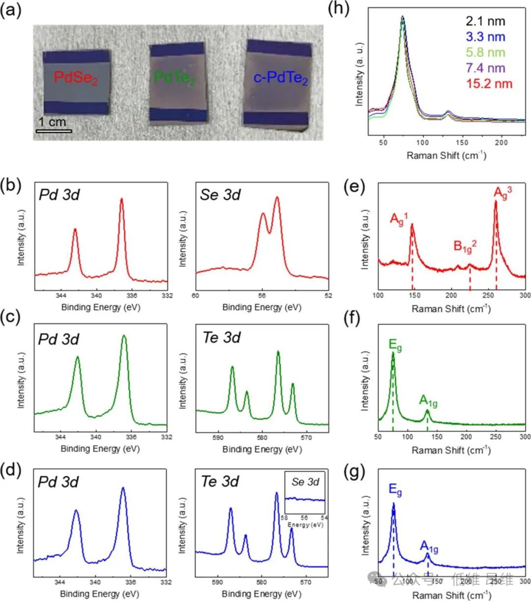 Figure 4. Anion exchange-driven conversion of 2D PdSe2 layers to 2D PdTe2 layers and their spectral characterization. (a) Images of prepared PdSe2 and PdTe2 layers and the converted (c) PdTe2 layer. (b)-(d): (b) XPS core-level spectra of prepared PdSe2, (c) prepared PdTe2, and (d) c-PdTe2 layers. (e)-(g): (e) Raman spectra of prepared PdSe2, (f) prepared PdTe2, and (g) c-PdTe2 layers.

Figure 5. Semiconductor-to-metal transition associated with the conversion of 2D PdSe2 layers to 2D PdTe2 layers. (a) Optical microscope images of patterned c-PdTe2 layers with different palladium thicknesses and the prepared PdSe2 layers. All scale bars in the images are 100 micrometers. (b, c) Comparison of the optical properties of prepared PdSe2 and PdTe2 as well as c-PdTe2 layers through (b) UV-Vis absorbance and (c) Tauc plot. (d) Ids-Vds curve obtained from the FET converted from thin PdSe2 layer (palladium thickness = 2.1 nm) to c-PdTe2 layer. (e) Ids-Vg curve of the same FET in (d) at Vds=1 V. (f) Comparison of Ids-Vds curves of c-PdTe2 FET with different palladium thicknesses at Vg=0 V. (h) Comparison of Ids ratios obtained from the prepared PdSe2 (blue) layer and c-PdTe2 (red) layer in field-effect transistors at Vg=±60 V with varying palladium thickness.

Figure 6. Application of anion exchange-driven semiconductor-to-metal transition in fully 2D PdSe2 layer-based flexible devices. (a) Schematic diagram of fully 2D PdSe2/c-PdTe2 planar heterojunction devices made using specific site anion exchange reactions. (b) Image of fully 2D flexible devices composed of SiO2/PdSe2 channels and c-PdTe2 electrodes. (c) Raman spectra obtained from the marked red and blue points in (b), showing the characteristics of PdSe2 (left) and PdTe2 (right). (d) Time-resolved broadband synaptic plasticity response under light pulses with a 0.5-second interval. (e) Time-resolved photoresponse under long intervals of 20 seconds and different intensity illuminations. (f) Photosensitivity related to illumination intensity.
References
Introducing Semiconducting-to-Metallic Transitions into Wafer-Scale 2D PdSe2 Layers by Low-Temperature Anion Exchange and Thickness Modulation
(ACS NANO.2024.DOI:10.1021/acsnano.4c11627)
Reference link:
https://pubs.acs.org/doi/10.1021/acsnano.4c11627?fig=tgr1&ref=pdf
Shanghai Angwei Technology Co., Ltd. provides two-dimensional materials such as single crystals and thin films as consumables, components and photolithography masks, and various testing and analysis services. We welcome all teachers and students to consult and strive to provide the best service.


