Source | https://blog.csdn.net/lxm920714/article/details/107942572
Recently, I designed a new board using the Spartan 7 chip to overlay an OSD menu on the front-end video source. The front-end converts HDMI to LVDS for the FPGA to process. During the schematic design phase, I did not carefully read the FPGA manual, which led to incorrect power supply for the LVDS BANK. It should be connected to 2.5V, but it was actually connected to 3.3V, and the BANK power supply was not isolated with a ferrite bead, resulting in the FPGA LVDS not functioning. I gathered relevant information and summarized it here to avoid making similar mistakes in the future.
1. Basic Introduction to HR and HP Banks
Xilinx’s 7 series FPGAs have two types of I/O Banks: HP (High Performance) and HR (High Range). The design of HP (high-performance) I/O banks aims to achieve higher memory and chip-to-chip transmission rates, while HR (high-range) I/O banks are designed for a wider range of I/O voltage standards. The I/O voltage of these two BANKs is different; the maximum VCCO voltage for HR I/O Banks is 3.3V, while for HP I/O banks, it is 1.8V. Especially for first-time users of the 7 series, it is crucial to pay attention to the maximum operating voltage of their I/O ports in hardware design. A careless mistake can lead to incorrect voltage, causing the FPGA to malfunction.
2. LVDS Levels of HR and HP Banks
When the I/O ports of the two banks are used as LVDS levels, the I/O voltage VCCO of HR banks can only be 2.5V, while the I/O voltage of HP banks is 1.8V. The LVDS standards supported by the two banks are different; HR I/O banks can only allocate to the LVDS_25 standard, while HP allocates to the LVDS standard.
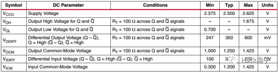
The DC characteristics of LVDS_25 are shown in the table below.
The DC characteristics of LVDS are shown in the table below.
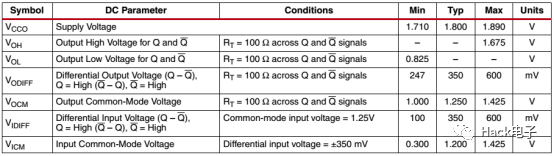
Comparing the two tables above, it can be seen that although the operating voltages of LVDS_25 and LVDS banks are different, the DC characteristics of the LVDS levels are the same. The LVDS operating voltage for high-speed AD/DA is generally 1.8V. When first using the 7 series, some hardware engineers may worry: since the operating voltage of the HR bank is 2.5V, can the LVDS of the HR bank be directly connected to the LVDS interface of the AD/DA with an operating voltage of 1.8V? By examining their LVDS DC characteristics, it can be concluded that it is safe to connect them directly.
3. Can LVDS Still Be Used if HR Bank Voltage is Incorrect?
As described above, for hardware engineers using the 7 series for the first time, when connecting the LVDS interface of the 1.8V operating voltage AD/DA to the FPGA, the designer mistakenly designed the I/O port voltage VCCO of the FPGA HR banks to be the same as the AD/DA I/O voltage of 1.8V. Due to not carefully reviewing the FPGA data manual, the design had flaws. When the circuit board was processed and returned, it was discovered that there was a design issue, causing anxiety. Such a basic error would surely be criticized by the leadership. At this point, do not panic; do not think about immediately redesigning. Instead, think about how to compensate for it. Even if full functionality cannot be guaranteed, at least some functions should be validated to ensure that this version of the circuit board has some value. This is the wish of most hardware engineers. I have encountered this issue and verified that even if the HR I/O voltage is designed to be 1.8V, it can still be used as LVDS. I also consulted Xilinx technical personnel, who confirmed that I/O voltage mainly affects the impedance matching of LVDS. Therefore, incorrect voltage will not guarantee that the LVDS rate reaches the theoretical rate; how much rate can be achieved depends on one’s “luck”.
Xilinx 7 series chips no longer support LVDS33 levels; under a VCCO voltage of 3.3V, the LVDS25 interface cannot be used.
Some designers attempt to configure it as LVDS25 in software while actually supplying 3.3V to achieve LVDS33, which is also ineffective. The reason is that Xilinx 7 series chips have added over-voltage protection in terms of I/O configuration, thus it is impossible to forcefully configure I/O by deceiving synthesis software. For more details, refer to the 7-Series SelectIO Resources Guide (https://www.xilinx.com/support/documentation/user_guides/ug471_7Series_SelectIO.pdf), page 100, Note 2 states:
“If the voltage exceeds 2.85V, the outputs will be in a high-Z state. The device should always be operated within the recommended operating range as specified in the 7 series FPGA data sheets.”
Although LVDS25 cannot be output under a VCCO of 3.3V, it can be used as an input. For more details, see AR#43989 https://www.xilinx.com/support/answers/43989.html
Even if the VCCO level is not 1.8V, LVDS input can still be used in the HP I/O bank. LVDS output (and thus bidirectional LVDS) can only be used for groups powered at 1.8V.
Similarly, even if the VCCO level is not 2.5V, LVDS_25 input can still be used in the HR I/O bank. LVDS_25 output (and thus bidirectional LVDS_25) can only be used for banks powered at 2.5V.
After checking the above statements, we conducted our own experiments:
Experimental Verification:
Bank 14 is an HR Bank, using differential input and output with LVDS levels:


Note: LVDS levels do not support HR bank.
Differential input and output using LVDS25 levels:
Note: VCCOs are contradictory; when outputting the differential clock sys_clk_out_p, VCCO=2.5V is required, but there is no such requirement for input.
Verification showed:
Even if the VCCO level is not 1.8V, LVDS input can still be used in the HP I/O bank. LVDS output (and thus bidirectional LVDS) can only be used for groups powered at 1.8V.
Similarly, even if the VCCO level is not 2.5V, LVDS_25 input can still be used in the HR I/O bank. LVDS_25 output (and thus bidirectional LVDS_25) can only be used for banks powered at 2.5V.
Official further explanation:
1. Xilinx Customer Community
https://www.xilinx.com/support/answers/43989.html
2. Xilinx Customer Community
https://forums.xilinx.com/t5/Design-Entry/spartan7-power-wiring-LVDS-25/m-p/984802
// Additional Note: LVDS in FPGA LVDS33 LVDS25
This is merely a naming convention. For XILINX FPGAs, LVDS25 means that the bank’s power supply voltage VCCO is 2.5V, while LVDS33 means that the bank’s power supply voltage VCCO is 3.3V. When using LVDS signals in code, the pins need to be constrained as LVDS25 and LVDS33 respectively. However!! The LVDS levels output by FPGA pins are all standard LVDS levels, generally with a common-mode voltage of 1.25V and a swing of 350mV. The following diagram is from the official ds926 manual provided by FPGA, which shows that LVDS25 and LVDS are merely named differently due to different VCCO, but the levels output by FPGA pins are all standard LVDS.
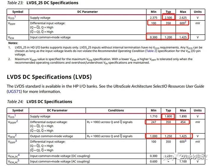
This can lead to some issues, as people often ask whether LVDS25, LVDS33, and LVDS chips (or FPGA constraints) can be compatible. The answer is yes, because most products on the market will only use one standard LVDS level, as mentioned above. Therefore, during this external interface, if the other party’s LVDS chip uses a 3.3V power supply voltage and claims their standard is LVDS33, while my FPGA generates LVDS signals in the HP BANK, I initially thought they were incompatible. However, after checking online resources and the manual of the chip used by the other party, I realized this issue. A small LVDS level problem was only understood when I encountered the issue today.
The difference lies only in the internal components.
LVDS33 requires a 3.3V Vcco, while LVDS25 requires a 2.5V Vcco (or for newer components, it may use Vccaux).
The signal interface on the pins is the same.
That is, the voltage swing and common-mode voltage are the same in both cases, so you can consider them as LVDS.