 Hello, welcome to the FPGA technology community. The community is vast, and meeting here is fate. You can follow the FPGA technology community to access other resources of interest in the “Adventuring in the Community” and “Chivalrous Acts” sections, or join us for discussions. The “Chivalrous Acts” section leads to the IC technology circle, where there are nearly 50 IC technology public accounts.
Part One: Design Overview
This design is a multi-channel UART/SPI communication system that enables one-to-many communication. The system can operate in UART mode or SPI mode. The reason I chose this topic is mainly that my current laboratory needs to develop fast communication based on UART. This topic can help me consolidate the knowledge I have learned before and prepare for my future projects. During the completion of this project, I mainly used knowledge related to FPGA state machines, buses, and other aspects. This project can be applied in scenarios requiring high-speed asynchronous or synchronous serial communication, such as real-time control and monitoring.
When the system operates in UART mode, a single transmitter can send information to up to four receivers, with the valid information containing an address code. The receivers can determine whether the information is intended for them based on the address code sent by the transmitter, achieving signal line multiplexing. UART communication is simple, requiring only one signal line; however, its drawback is that it can only achieve unidirectional communication, meaning the receiver cannot send data back to the transmitter. This limitation can be mitigated by using two UART systems.
When the system operates in SPI mode, communication can occur between one master and multiple slaves, and the communication is full-duplex. The master selects a slave by pulling down the chip select signal of one or more slaves.
Part Two: System Composition and Function Description
Planned Functions
The program implements communication for both UART and SPI, and allows switching between the two modes via a button. In UART mode, the transmitter sends a string of data to the receiver, which checks if it matches known data. If it matches, an LED lights up; if not, it remains off. In SPI mode, the master and slave send data to each other simultaneously. If the received data matches known data, an LED lights up; if not, it remains off. Both UART and SPI have addressing capabilities. The addressing method for UART adds two address bits before the data bits to distinguish up to four receivers; the addressing method for SPI pulls down the SS signal of the selected slave to distinguish up to four receivers.
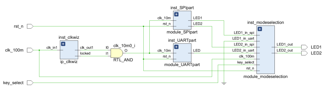
Currently, all functions have been implemented. The initial plan was to implement the communication system on two different FPGA boards, but one of the boards had issues, so validation can only be done on one board. The transmitter, receiver, master, and slave are all written on one board, and the internal communication lines are directly connected using the internal lines of the FPGA. The overall block diagram is as follows. Here, inst_clkwiz is the built-in frequency divider of the system, which reduces the external 100M signal to 10M, lowering the communication rate but making the communication system more stable; inst_SPIpart is the SPI communication module; inst_UART is the UART communication module; inst_modeselection is the communication mode selection module.
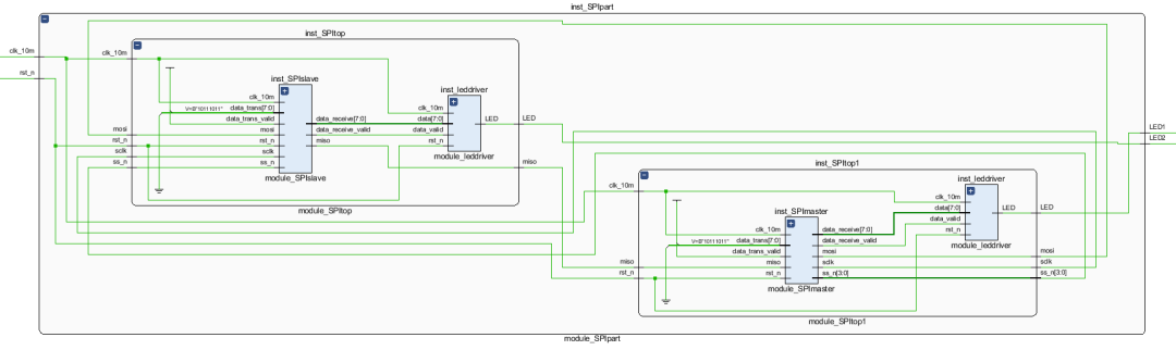
The internal structure of SPI is as follows. Here, inst_SPItop is the slave; inst_SPItop1 is the master. When the master’s signal selection is 0111, the slave in the system is selected. Inside the master and slave, inst_SPImaster is the SPI master port, inst_SPIslave is the SPI slave port, and inst_leddriver is the LED driver circuit, responsible for checking if the received signal matches the known signal. When the received signal matches the known signal, it drives the LED to light up.
The block diagram of the UART part is as follows. Here, inst_UARTtop1 is the transmitter; inst_UARTtop is the receiver. The transmitter sends data to the receiver. When the receiver receives data that matches the known data, it drives the LED to light up.
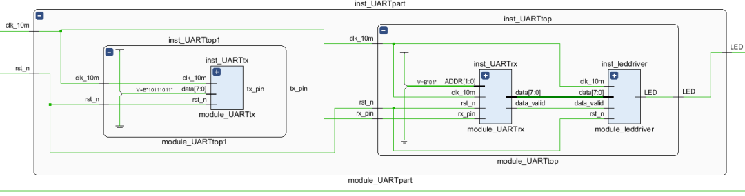
Part Three: Completion Status and Performance Parameters
All functions can be implemented on one board, except for communication between two boards.
Testing Method:
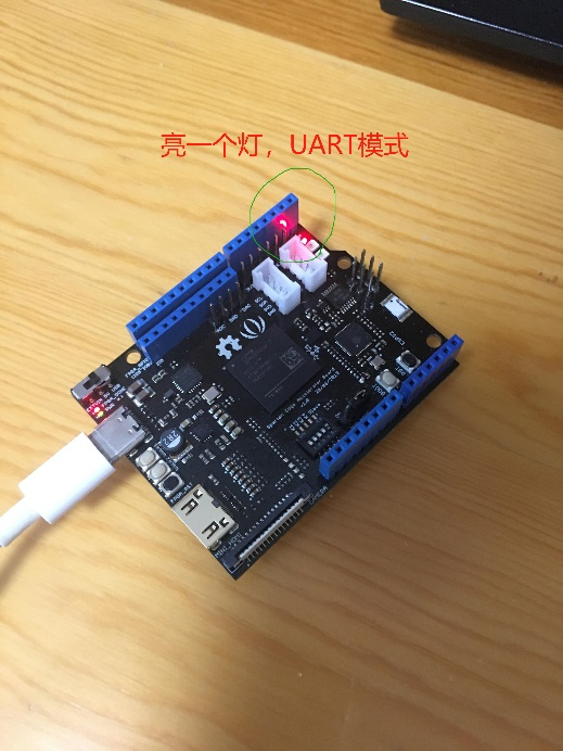
After powering on, first press RST to reset the board. The default communication mode after reset is UART mode. The red LED lights up, indicating that in this mode, the receiver has completely received the ten-bit signal and completed the address check. After passing the received signal to the LED driver module, it is determined to match the known data 8’hbb. LED2 is set, lighting up the red LED2, while in UART mode, the green LED1 remains off. Based on these observations, the UART mode is operational.
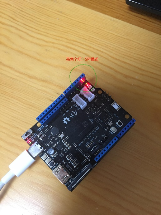
Pressing KEY1 lights up both the red and green LEDs, with the green LED being dimmer than the red LED. The red LED indicates that the master has successfully selected the slave, sent data to the slave, and the slave has received the data from the master, which matches the known data after passing through the LED driver module. The green LED indicates that the slave has also successfully sent data to the master, which also matches the known data. The reason the green LED is dimmer than the red LED is that the master only connected one slave, so it only receives matching signals 1/4 of the time, while during the other 3/4 of the time, it receives 8’bzz, which does not match the known signal, keeping the LED off. Therefore, the brightness is lower.
Pressing KEY1 again switches the system back to UART mode, turning off the green LED and lighting up the red LED.
Selected Past Articles


[Free] FPGA Engineer Recruitment Platform
FPGA talent recruitment, HR from companies, take note!
Selected System Design | Design of Real-Time Image Edge Detection System Based on FPGA (with code)
Design of Gigabit Ethernet RGMII Interface Based on Primitives
Theory of Timing Analysis and Use of TimeQuest – Chinese Electronic Version
Job Interview | Latest Compilation of FPGA or IC Interview Questions
Resource Compilation | FPGA Software Installation Packages, Books, Source Code, Technical Documents… (Updated 2025.02.19)
FPGA Employment Class starting July 19, online and offline, systematic learning, one-on-one online tutoring, lifelong technical support!
FPGA Technology Community Broadly Invites Posts
No ads, pure mode, providing a clean space for technical exchanges, from beginners to industry elites and big names, covering various fields from military to civilian enterprises, from communication, image processing to artificial intelligence, all directions are available. QQ and WeChat options, FPGA technology community creates the purest and most professional technical exchange and learning platform.
FPGA Technology Community WeChat Group

Add the group owner’s WeChat, note your name + school/company + major/position to join the group
FPGA Technology Community QQ Group

NoteName+School/Company+Major/Position to join the group
