DAC Model: ES7148.
Package: QFN12.
Operating Temperature: -40~+85℃.
1. Overview
The ES7148 is a 12-pin, 24-bit stereo D/A converter that uses PCM (Pulse Code Modulation). It supports 24-bit word length I2S serial audio data format input. Utilizing multi-bit ∆-Σ modulation technology, it converts digital signals to dual-channel analog signal output. The multi-bit ∆-Σ modulator makes the ES7148 less sensitive to clock jitter and reduces out-of-band noise.
Sampling Frequency: 200KHz
Supports USB clock or non-standard audio clocks, such as 25 MHz or 26 MHz.
I2S audio data format, 16-24 bits.
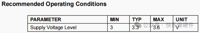
Powered by a single supply of 3~3.6V.
2. Functional Block Diagram
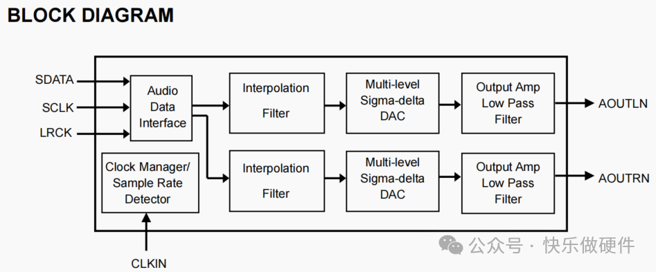
SDATA is the serial audio data input; SCLK is the data clock; LRCK is for selecting the left and right channels.
CLKIN is the system clock.
Clock Manager/Sample Rate Detector is for clock management and sample rate detection.
Audio Data Interface is for audio data interface; Interpolation Filter is for interpolation filtering;
Multi-level Sigma-delta DAC is for the multi-bit ∆-Σ modulation DAC module;
Output Amp Low Pass Filter is for low-pass filtering output.
AOUTLN is the left channel analog data output; AOUTRN is the right channel analog data output.
3. Pin Description
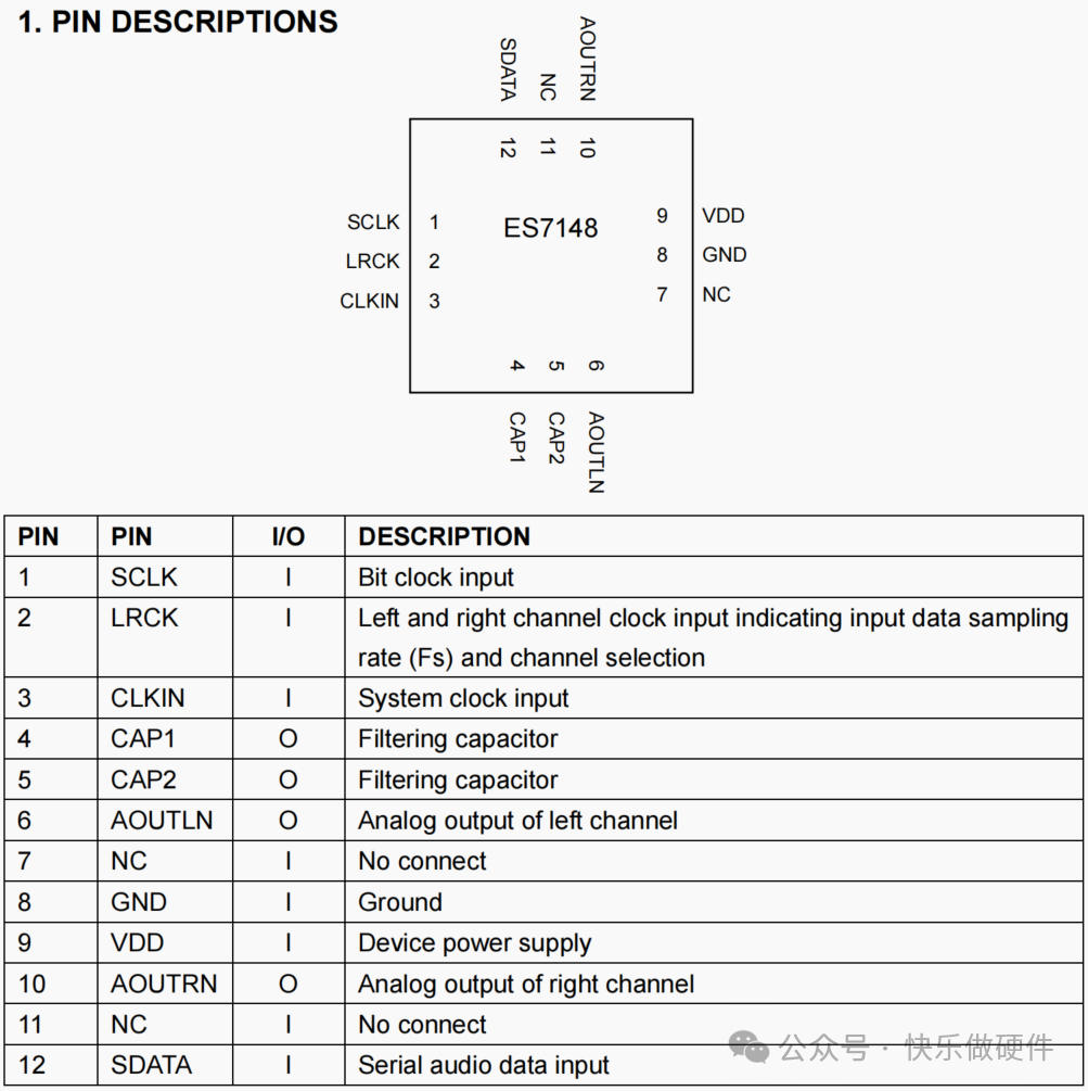
Pin1_SCLK, data clock input.
Pin2_LRCK, left and right channel clock input, indicating the input data sampling rate (Fs) and channel selection.
Pin3_CLKIN, system clock input.
Pin4_CAP1, filter capacitor.
Pin5_CAP2, filter capacitor.
Pin6_AOUTLN, left channel analog output.
Pin7_NC, not connected.
Pin8_GND, ground.
Pin9_VDD, system power supply.
Pin10_AOUTRN, right channel analog output.
Pin11_NC, not connected.
Pin12_SDATA, serial audio data input.
4. Recommended Application Circuit
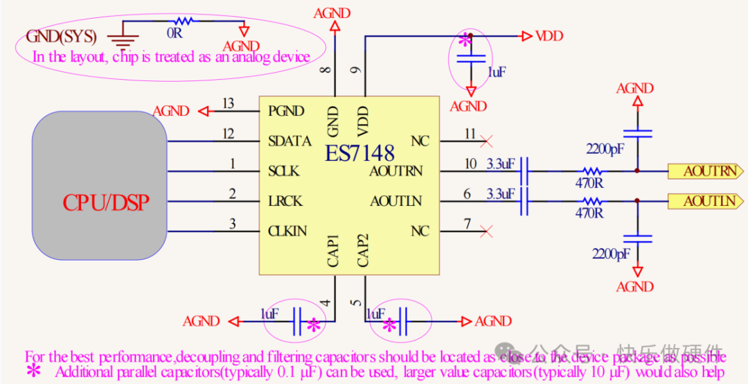
When laying out, treat the ES7148 chip as an analog device.
Decoupling and filter capacitors should be placed as close to the ES7148 as possible. Additional parallel capacitors (typically 0.1μF) and larger value capacitors (typically 10μF) can also be used.
Note: The ES7148 does not support differential output, only single-ended output or pseudo-differential output.
5. Application Description
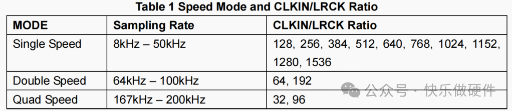
5.1 Sampling Rate and Input Clock
According to the sampling rate, the ES7148 can operate in three modes: single-speed, double-speed, and four-speed. The ES7148 supports using USB clock or non-standard clocks.
5.2 Audio Data Input
The ES7148 can receive 16~24 bit I2S serial audio data and can automatically detect the data word length. The following figure shows the relationship between SDATA, SCLK, and LRCK.
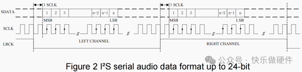
When LRCK is low, the ES7148 activates the left channel;
When LRCK is high, the ES7148 activates the right channel.
5.3 Power Up and Down
After power-up, the ES7148 will self-reset and enter power shutdown mode. In this mode, the ES7148 clamps the output to ground and shuts down all internal circuits except for the clock management unit. Once it receives the appropriate system clock CLKIN and left-right channel switching signal LRCK, the ES7148 will exit power shutdown mode, output a common-mode voltage, and enter normal operating mode.
6. Electrical Performance
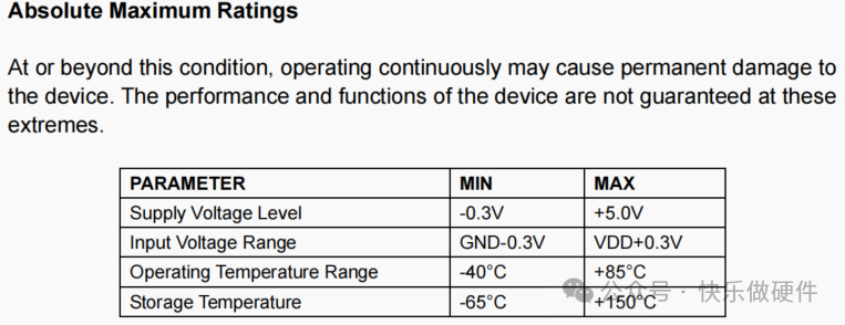
6.1 Maximum Ratings
6.2 Recommended Operating Conditions
6.3 Analog Characteristics
Test conditions: VDD=3.3V, GND=0, ambient temperature=25℃, Fs=48KHz, CLKIN/LRCK=256, input 0dB 1KHz sine wave.
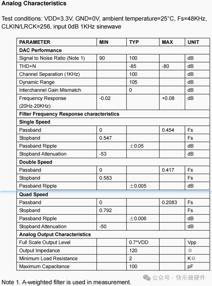
DAC Performance
Signal-to-noise ratio: 90dB (Typ.)
THD+N: -85dB (Typ.)
Channel isolation: 100dB (Typ.)
Dynamic range: 105dB (Typ.)
Channel gain mismatch: 0dB (Typ.)
Frequency response: -0.02~+0.08dB
Filter Frequency Response Characteristics
Single-speed, double-speed, four-speed:
Passband, stopband, passband ripple, stopband ripple
Analog Output Characteristics
Full-scale output level: 0.7*VDD (Typ.)
Output impedance: 120Ω (Typ.)
Minimum load resistance: 2KΩ (Typ.)
Maximum capacitance: 100pF (Typ.)
Note 1: An A-weighted filter was used during testing.
6.4 Serial Audio Interface Switching Characteristics
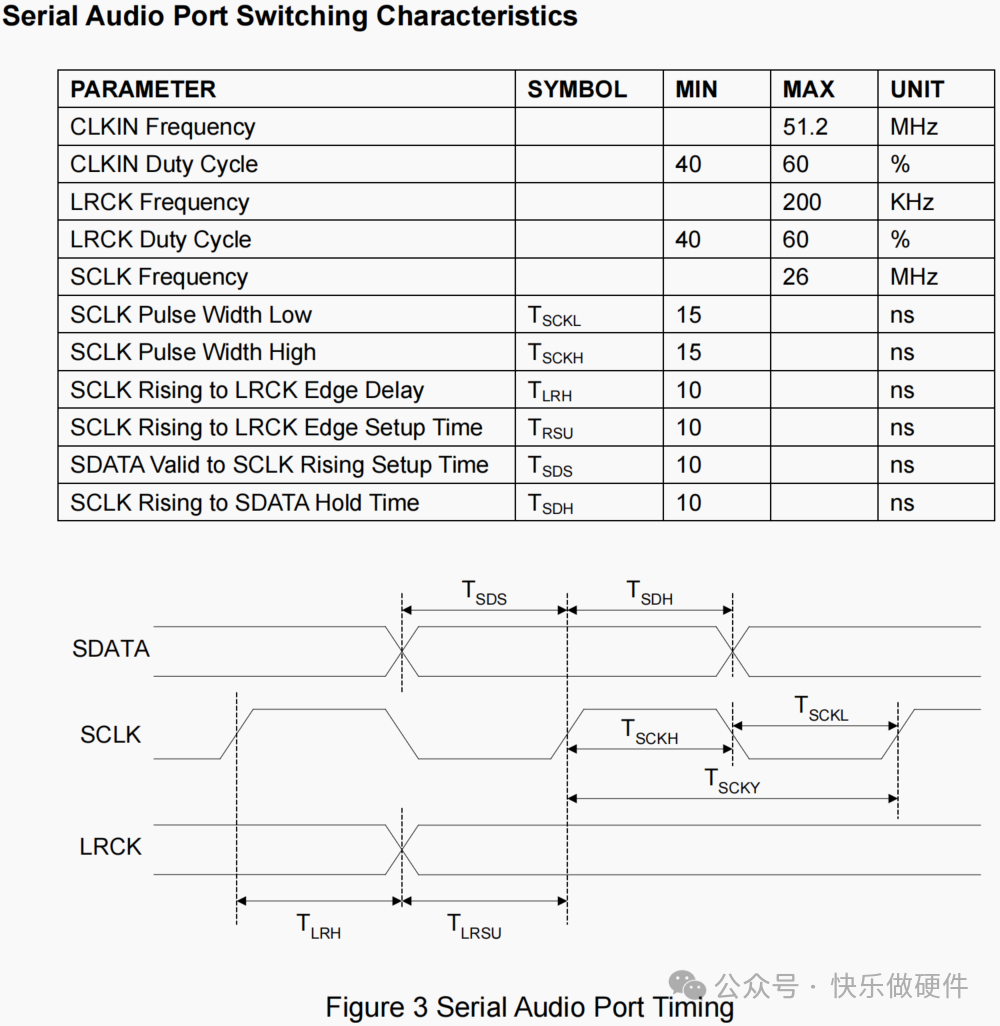
System clock CLKIN frequency: 51.2MHz (Max.)
System clock CLKIN duty cycle: 40~60%
Left and right channel clock LRCK frequency: 200KHz (Max.)
Left and right channel clock LRCK duty cycle: 40~60%
Data clock SCLK frequency: 26MHz (MAX.)
Data clock SCLK low pulse width Tsckl: 15ns (MIN.)
Data clock SCLK high pulse width Tsckh: 15ns (MIN.)
Data clock SCLK rise to left-right channel clock LRCK edge delay time Tlrh: 10ns (MIN.)
Data clock SCLK rise to left-right channel clock LRCK edge setup time Trsu: 10ns (MIN.)
Serial audio data input SDATA valid to data clock SCLK rise setup time Tsds: 10ns (MIN.)
Data clock SCLK rise to serial audio data input SDATA edge hold time Tsdh: 10ns (MIN.)
6.5 DC Characteristics
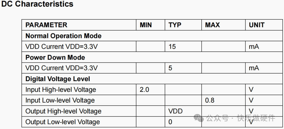
Normal Mode
Current at VDD=3.3V: 15mA (TYP.)
Power Shutdown Mode
Current at VDD=3.3V: 5mA (TYP.)
Digital Signal Levels
Input high level: 2.0V (MIN.)
Input low level: 0.8V (MAX.)
Output high level: VDD (TYP.)
Output low level: 0V (TYP.)
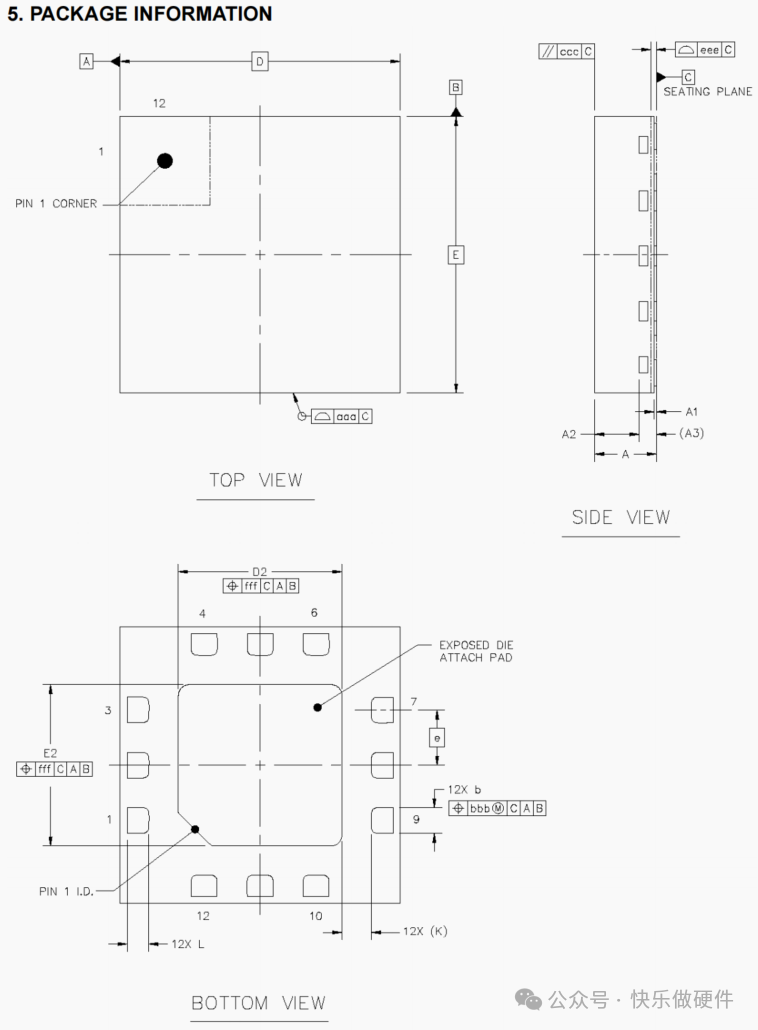
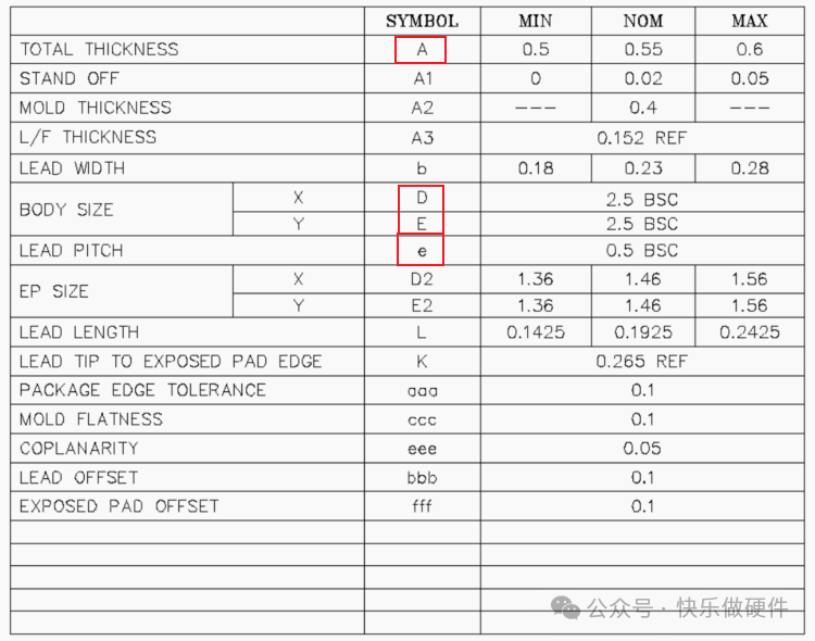
6.6 Package Information
ES7148 Package: QFN12
ES7148 Dimensions: 2.5*2.5*0.55mm
Pin Pitch: 0.5mm