For beginners in electronic technology, mastering basic circuit principles, the functions and characteristics of components, how to analyze circuit diagrams, reading PCBs, soldering techniques, and common troubleshooting methods are all essential skills that need to be well understood. This article discusses how to read PCBs, hoping to assist beginners.
PCB stands for printed circuit board, and the layout of components on a PCB often differs significantly from the schematic diagram, which can confuse beginners and make it difficult to see the connections. However, once you read through the PCB analysis tips below and practice, you will be able to understand it clearly.
2. Next, identify components based on their markings, which usually indicate certain parameters or model numbers. They may also include manufacturer information, batch numbers, version numbers, and sometimes even symbols for international certifications. This method also relies on your familiarity with component models and parameters.
For example, a transistor marked as C1815 is a low-power, low-frequency NPN transistor; TL431 indicates an integrated voltage regulator IC; and 13001 denotes a small power switching transistor, which can be used in small power chargers.
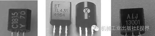 Figure 1: Components that look similar but are labeled C1815, TL431, and 13001
Furthermore, you can disassemble components to examine their internal structures. This practice is encouraged, as the more you disassemble, the more familiar you become with the internal structure and working principles of components. You can disassemble as many components as possible to enhance your basic knowledge of electronic parts.
3. If a component is on the PCB, you can determine its type based on the component symbols and silkscreen on the PCB. For instance, if it is labeled R12, it is a resistor numbered 12 in the circuit. X, Y, and Z can denote crystal oscillators, and you can also infer the component’s function based on its circuit context, which requires familiarity with basic circuits.
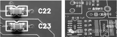
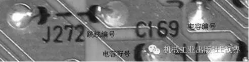
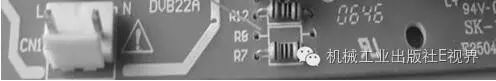 Figure 2: Various component symbols, numbers, and parameters on the circuit board
Due to technology, production, and manufacturer differences, the same type of component can vary in shape, structure, and materials, which may complicate your PCB analysis. If conditions allow, visit specialized electronic component stores and electronic markets to learn more, as this greatly aids in your knowledge accumulation.
(1) When the power is connected and the gas is opened, turn on the hot water valve;
(2) At this point, the water flow sensor detects the flow rate and sends this information to the mainboard CPU; after reaching a certain flow rate, the CPU sends out related control signals. These signals may appear as a water flow indicator on the display, control the fan drive circuit, and start timing, etc.
(3) After the fan drive circuit operates, it outputs DC power voltage and fan speed control voltage to the fan, causing the DC brushless motor to operate;
(4) When the motor reaches a certain speed, the Hall element circuit inside the motor detects the actual speed and sends it to the mainboard CPU. When the CPU determines this value, the control circuit powers the ignition transformer to perform high-voltage discharge ignition.
(5) After a certain ignition time, the CPU then controls the circuit to provide the gas proportioning valve with the highest DC voltage, causing the valve to open to its maximum position. At the same time, it controls the segmented proportional valve, fully opening the gas channel and igniting the gas in the combustion chamber under ignition. At this point, the display will show a burning indicator.
(6) The flame ignites the flame detection electrode, and the circuit detects the combustion information and sends it to the CPU, which recognizes the successful ignition of the water heater and maintains a series of output voltages to keep the fan, solenoid valve, etc., operational.
(7) During ignition, the segmented proportional valve operates fully, and after ignition, it selectively energizes certain segments based on the set temperature. At the same time, the gas proportioning valve reduces its working voltage from the highest to a rated voltage, effectively reducing the valve opening.
(8) If the ignition process is abnormal, whether the fan does not turn or there is no ignition action, or if the flame goes out after igniting, the CPU will recognize this and display the corresponding alarm code on the screen. Of course, if the water heater has defective components that are within the CPU‘s startup self-check range, the display will also show fault codes upon power-up.
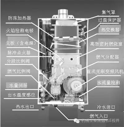 Figure 3: Structure of a high-end balanced gas water heater
The above describes the working process of a balanced gas water heater. If it is a conventional forced exhaust gas water heater, its working process is much simpler. Due to the different structures and components of forced exhaust gas water heaters, the working process also differs from that of balanced gas water heaters. Below is a brief description of the working process for forced exhaust gas water heaters.
Power on, open the gas valve, then open the hot water valve; the water-gas linkage valve will move radially to the left under the pressure of the water flow, pushing the mechanical water switch open (some use reed switch type water switches), while simultaneously opening the gas shut-off valve’s rubber ring. The control box receives the information from the water switch and activates the relay to power the 220V AC fan.
The wind pressure generated by the rotating fan activates the wind switch connected to the gas pipe; after the control box receives the operational information from the wind switch (the wind switch has normally closed and normally open terminals, mostly using normally open contacts), it ignites the igniter, which outputs high-voltage pulses for ignition. At the same time, the control box outputs a voltage to energize the gas solenoid valve, allowing the gas channel to flow freely and igniting at the burner outlet. Once ignition is successful, the flame detection electrode heats up, and once detected by the control box, it continues to output a series of voltages to keep the fan and solenoid valve operational for combustion.
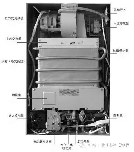 Figure 4: Internal structure of a balanced gas water heater
The ignition process of water heaters, especially forced exhaust gas water heaters, can be visually observed by removing the casing. Understanding the working process of an electrical appliance or its workflow not only includes the functions and working principles of the key components but also guides our troubleshooting and repair thought processes.
Of course, once you understand the working process of an appliance, if a fault occurs, most of the time you only need to pay attention to the fault phenomenon, i.e., which step of the process it has reached, without needing to use a multimeter to measure, allowing you to analyze and judge which part has a problem. For example, if the water heater sounds like the fan is running but there is no ignition sound afterward, simply sending the wind pressure switch signal to the control box can easily identify the fault location.
Learning and hands-on practice, if we pay more attention and think critically, can lead to unexpected gains. Especially when we understand the working process of an appliance, many related knowledge aspects are included; the question is whether we are adept at discovering them.
2.It is best to first observe the power supply and ground wire routes, while noting down those power and ground wires. When you analyze components, if one end connects to power or ground, you can consider that section of the circuit complete.
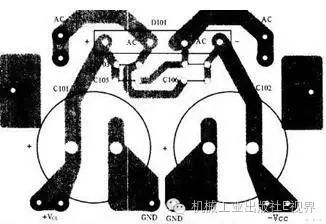 Figure 5: Power circuit of an amplifier
The edge of the circuit board, the largest copper foil strip, and the copper connection points of the heat sink are generally the negative, i.e., ground wire. (However, some high-power components may not connect to ground.) If these features are not obvious, you can look at the power filtering capacitor (for the positive power supply), where the negative terminal of the electrolytic capacitor connects to the circuit’s negative or ground wire.
Regarding power supply and ground wire, in some electronic products, there may be several separate power supplies for the circuit, and there may also be multiple ground wires that may not be interconnected. For example, the primary and secondary grounds of a switching power supply: the primary ground is commonly referred to as hot ground, connected to the 220V power supply and carries voltage; the secondary ground is called cold ground and does not carry voltage.
3.It is recommended to follow the signal flow when observing PCBs, either forward (e.g., starting from the high-frequency head) or backward (e.g., starting from the speaker) is acceptable; sometimes a combination of both approaches is suitable for analyzing certain circuits.
Circuit branches are inevitable, and when this occurs, you should examine each branch separately. If there are too many branches, you can mark them to distinguish the ones you’ve already reviewed, and you can pause at marked points to examine other branches or circuit sections. When you return to the original paused point, you can consider the analysis of that circuit complete.
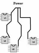 Figure 6: Branching of power supply
4. When following the signal flow, upon encountering a unit circuit or functional circuit,you should analyze it centered around core components such as transistors and ICs, examining the components and connections associated with each pin of the transistor and the surrounding components and circuits of the IC.
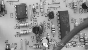 Figure 7: Centering analysis around chips and transistors
Of course, you can also break down the entire board into sections for analysis. You can analyze the functions of components while observing how signals change, considering the potential faults that could arise from component damage, which is better. When encountering unfamiliar circuits, clarify their structure and characteristics, then relate them to similar typical circuits for comparison and analysis.
5.It is best to prepare a soldering iron and multimeter when examining PCBs. Because when encountering a transistor, you must know whether it is an NPN or PNP type, as well as the pin arrangement, to analyze the circuit; otherwise, the significance of the analysis diminishes, leading to considerable doubts and errors. Therefore, transistors should be measured, and some other components may also require measurement.
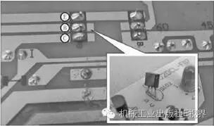 Figure 8: Transistor with marked pins
As you gain more experience and knowledge, you may not need to measure while examining most PCBs, judging the type of transistor and the arrangement of its electrodes based on the circuit paths and the connected components and functional circuits.
For instance, an NPN transistor that serves a control function generally has its emitter connected to ground, the base connected to a control input signal, and the collector connected to the controlled component. For example, the collector of the transistor connects to pin 2 of an optocoupler and the coil winding pin of a relay (while also connecting to the positive terminal of a diode).
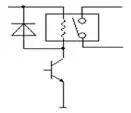 Figure 9: Understanding the circuit helps determine transistor polarity and pin arrangement
Similarly, for assembly machines (CRT TVs) using switch-mode power supplies, which adopt a four-transistor discrete form, based on our previous knowledge of transistors, we know the voltage relationships of each pin when the transistor operates normally. For instance, in a common-emitter or common-collector circuit powered by a positive supply, the emitter of an NPN transistor connects to a low potential, while the collector of a PNP transistor connects to a low potential, with the base being the signal voltage input.
By observing the power supply, we find that the first pin of the first transistor connects to the +300V resistor drop (i.e., high potential), the third pin connects to pin 4 of the optocoupler, and simultaneously connects through a resistor to the first pin. The second pin connects to pin 3 of the optocoupler, while also connecting to one pin of another transistor, and the last pin connects directly to ground. From this, we can determine that the first transistor is a PNP type with pin arrangement E, C, B; the other transistor is an NPN type with pin arrangement B, C, E.
 Figure 10: Transistors outlined
Regarding this example, it may be somewhat difficult to understand. When describing it, you need to combine the circuit diagram and knowledge of transistors while fully exercising your imagination to keep pace. You might wonder why the first transistor is not an NPN type and why the pin arrangement is C, E, B? This perspective suggests that your analysis must be correct in identifying the third pin as the base. However, upon closer examination, this assumption seems flawed. First, transistors rarely have such pin arrangements; second, for an NPN transistor to serve as a control element, it is generally used with the collector.
Sometimes you also need to identify the connection relationships and working principles based on the internal structures of components (such as switches, potentiometers, and transformers), which requires measurement. For double-sided boards (multi-layer boards), components often cover some wiring and vias, making it necessary to measure or even disassemble components to observe them directly.
6.Beginners must draw the schematic diagram while examining PCBs, marking each component with its number to avoid missing, misinterpreting, or overlooking components, and correcting errors promptly.
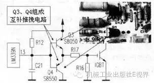 Figure 11: Drawing the schematic while examining the PCB
Initially, when observing PCBs, you can find similar schematics (minor differences are okay) to analyze and compare.
 Figure 12: Finding a similar schematic when examining the induction cooker circuit board
7. Components on the front side (for single-sided boards, but some surface-mounted components may be on the back) have traces and pads on the back. Remember that when you identify something on the front, it will be in the opposite direction on the back. For example, a capacitor on pin 1 of an IC (assuming it is on the left) will be on the right side of the IC on the back.
8. Some PCBs are designed for easier analysis, with blue, green, or brown bands printed on the front that match the positions of the copper foil strips on the back, along with component outlines and numbers; or on the back (for single-sided boards) printed with component symbols and numbers. For such boards, the former allows most of the circuit to be analyzed from the front, while the latter allows almost the entire circuit to be analyzed from the back, avoiding the hassle of flipping the board back and forth and reducing identification errors.
 Figure 13: The blue band on the front and the component outline on the back
9.There are also some experiences to draw from: for example, if a rectifier diode is about 10mm long and horizontal on the front, it will remain horizontal on the back, just with its polarity reversed. To find the component’s pads and pinholes on the back, you can first look at the approximate location, then check for two holes about 10mm apart and slightly larger than the diode’s pins; if no other diodes are nearby, those holes are for that component.
This means that when locating the pinhole positions of back-mounted components, you can use certain characteristics of the components and their relative positions to make judgments. If components are arranged in a regular grid, and you see a diagonal hole that seems to correspond to two pins, you might mistakenly think they belong to a component unless that component is specifically designed to be diagonal. For double-sided boards, the top and bottom layers are connected through vias.
When you enter the workforce or if you are already working in this field, as a skilled worker, you will need to maintain, repair, improve, and design electronic products, so mastering this skill is essential. Therefore, during your learning period, you should focus on training in the skill of drawing circuit schematics.
The specific process can begin with some simple and familiar boards for practice, before progressing to more complex ones.
 Figure 14: Simple and easy-to-understand circuit
For instance, start with basic amplifier circuits or series voltage regulator circuits. Just as one practices typing on a computer, where one letter may need to be practiced hundreds of times, the same applies to learning electronic technology. While not requiring that many repetitions, only through extensive practice can you become familiar with and understand the material. Only through repeated practice and summarizing and refining your experiences can you lay a solid foundation.
Like analyzing PCBs, we should also prepare a multimeter and soldering iron, primarily to clarify the types and polarities of some components, as well as the relationships of certain component pins.Next, prepare paper and pencil, as using a pencil allows for easier corrections. Finally, having a ruler will help in creating a neat, standardized, and coordinated schematic during the second draft.
When you are new to electronic technology, facing a densely packed PCB with intersecting lines, how can you accurately and quickly draw the corresponding circuit schematic? Therefore, regarding how to convert PCBs into schematics, what details should you pay attention to? Please see the following process interpretation.
1. It is recommended to reasonably divide the entire PCB into several functional areas
When drawing a schematic for a complete PCB circuit board, generally, components of the same functional circuit are concentrated in one area. Dividing the board by function can make drawing the schematic easier.
However, this functional area division is not arbitrary; it requires readers to have a certain understanding of electronic circuit knowledge. First, identify the core components of a specific functional unit circuit, then trace the connections and refer to related similar schematics to find other components in the same functional unit, forming a functional zone. The formation of functional zones is the basis for drawing schematics.
Additionally, during this process, do not forget to cleverly utilize the component numbering on the circuit board. Some designs use different numbering types for different functional circuits, such as C102, C111, V101 in one functional circuit; while V201, R203, D201 are in another functional circuit; and L502, V501, IC501, C503 are part of another functional circuit. Such numbering can help us quickly establish functional zones.
2.Identify core components
The core component is the primary part relied upon when starting to draw the schematic. Once the core components are determined, you can draw based on their pins, ensuring greater accuracy in the schematic.
For readers, identifying core components is not a complex task. Generally, you can select components that play a significant role in the circuit as core components, which are typically larger and have more pins, such as integrated circuits, transformers, and transistors.
3. Accurately and reasonably draw the lines
(1) First, check how many power supplies there are, then draw several power lines at different positions based on the circuit conditions. In the schematic, any functional circuit connected to power can be directly drawn to the corresponding power line. Distinguishing between ground wires, power lines, and signal lines also requires relevant knowledge of power supplies, circuit connections, and PCB wiring. This differentiation can be analyzed based on the component connections, copper foil widths, and the characteristics of the electronic product itself, or confirmed through measurements to determine the relationships between power and ground lines.
(2) While drawing the schematic from the PCB, each component drawn must be assigned the same number as on the PCB to facilitate error detection later on, ensuring that no components are misnumbered, duplicated, or omitted. If the components on the PCB are also marked with parameters and models, it is best to include these on the corresponding schematic components.
(3) Additionally, for beginners, it is advisable to mark the parts of the PCB that have been converted into the schematic. Many beginners tend to redraw components they have already sketched.
(4) Make full use of the Chinese and English labels on the PCB, such as IN, OUT, L, R, ON/OFF, to facilitate understanding of the circuit functions and drawing comparisons, as well as better circuit function classification.
(5) If a line is long or several lines run parallel, it is easy to misread; this is where the accuracy of the multimeter measurement comes into play. For multi-position switches, certain multi-position potentiometers, transformers, etc., you should also use the multimeter to determine their internal structures to understand the pin connections on the PCB, ensuring accurate schematic conversion. In any case, make extensive use of the multimeter’s measurement functions.
(6) For single-sided boards, surface-mounted components may cover the copper foil lines, or on double-sided boards, components may cover parts of the copper foil lines on the front, obstructing the analysis of the copper foil line paths and connections. Therefore, you may need to desolder those components that block your view.
(7) Since you have divided the PCB into functional areas, you can also draw the schematic by functional circuit, then connect them to form a whole.
The method for drawing unit functional circuits is: first draw the power supply, ground wire, signal input and output terminals, and core components. The power supply should be at the top, the ground at the bottom, the signal input on the left, the signal output on the right, and the core component in the center. Then draw other related components in that functional circuit. If the core component is an IC, you can first sketch an IC with the same number of pins, then draw the components connected to each pin.
(8) If you encounter significant confusion regarding the connections of a component or several components, pause at that point and mark it on the PCB. When you analyze other components and return to the original paused point, you will have completed the drawing of that segment.
(9) To determine whether a point or line is connected to a power supply or ground, you can use a multimeter to measure. When you become overwhelmed or fear making mistakes, measurement becomes even more essential.
(10) In wiring drawings, to avoid crossing and intertwining lines, you can draw a circle for the power supply and label it +5V, indicating this point is connected to the +5V power supply line. Ground wires can use grounding symbols to indicate those points are connected to the ground.
(11) Different functional lines can be drawn using different colors or line thicknesses for clear differentiation.
(12) For some circuits, you can also use a bus method to simplify the circuit. For instance, if a chip has five pins for detection functions, you can extend those pins and label them 1, 2, 3, 4, 5, then draw a large bracket and label it with representative letters or alphanumeric combinations. If these five pins connect to five temperature probes, you can draw the symbols for the five temperature probes on the side and label them 1, 2, 3, 4, 5, then draw a large bracket, marking it as N1. This bus method can reduce the number of connections in the middle, representing the connections between two or more corresponding points.
(13) For complex circuits, you can mark a point or line at both ends with the same attribute label to indicate a connection, thus avoiding intermediate connections. For example, if a line is broken, draw a circle and label it LPN; at the corresponding connection point, also label it LPN, indicating these two lines are connected.
If you are dealing with a double-sided PCB, which has copper foil lines on both sides, and components installed on one or both sides, compared to single-sided boards, double-sided boards have densely arranged components and more connections, making the wiring more complex, with finer copper foil lines and connections between the two sides through vias, increasing the difficulty of identification. However, do not worry; once you master the methods, you can conquer those difficulties through diligent practice.
4. Familiarize yourself with the basic circuit frameworks and structure diagrams while referring to similar and related schematics
Readers need to be well-versed in the basic frameworks and drawing methods of some electronic circuits. Not only should you be able to directly draw the basic compositions of simple, classic unit circuits, but you should also be able to form an overall framework of electronic circuits.
On the other hand, similar types of electronic products have certain similarities in their schematics. We can draw from our accumulated experience to refer to similar circuit diagrams for analyzing new product schematics.
5. Verify and optimize the drawn schematics
After completing the schematic drawing, it should go through a verification phase to check for errors in the drawing.One method is to count the number of components on the PCB and then compare it with the number of components in the drawn schematic. If there is a discrepancy, it indicates an error.
Once the component counts are verified, the next step is to check whether the connections are correct and whether the labels match. This process requires careful attention, ideally performing two comparisons.
After eliminating all errors, the next step is to optimize the schematic. Of course, if your drawn schematic has no errors, that’s even better. Optimization can refer to the drawing methods of other related schematics. Adjust the schematic until it is reasonable, standardized, accurate, and clear.
The basic principles for optimizing schematics are as follows:
(1) Circuits of the same function are generally drawn in a relatively unified position.
(2) The power supply should be drawn on the left or top; signal inputs on the left or top; signal outputs on the right or bottom, meaning the signal flow generally goes from top to bottom, left to right.
(3) If possible, draw ground lines on the same horizontal line, and you can have several horizontal lines to standardize the ground.
(4) Some components may appear in different parts of the circuit; if you are unclear about certain component symbols and labels, look up the data to see their standard drawings.
(5) The orientation of the same type of component should be determined based on the circuit form to decide whether to draw it horizontally or vertically for better aesthetics.
(6) Components of the same type in the same functional circuit should be aligned horizontally or vertically; other components not related to that circuit should also be aligned in the same direction if possible.
(7) Using the size of one component as a reference, other components can be drawn in proportion to it, making the layout more visually appealing, while also ensuring a moderate density between components.
Select several common circuit forms of PCBs to analyze and convert them into corresponding schematics.
In summary, regularly familiarizing yourself with common typical circuit diagrams can help us quickly draw circuit schematics and further analyze their working principles.
Converting PCBs into schematics requires comprehensive knowledge and skills. First, you need to have accumulated knowledge regarding electronic component identification and measurement.
Imagine if more than half of the electronic components on the PCB are unfamiliar to you, and you do not know their circuit symbols; you would not be able to start drawing the circuit schematic.
Mastering knowledge relies on broad exposure and accumulation, as well as careful observation and critical thinking. During the learning and working processes, in-depth communication and discussion with others are very necessary.
(-END-)
Selected from “Crossing Thinking, Electronic Technology Reader”

Previous Highlights
Absolutely classic! Application examples of external devices for microcontrollers
Classic microcontroller entry! 25 project materials available for free!