To make a simple 16-bit CPU, we first need to clarify what a CPU does. We should understand the composition of a computer (or its alternatives, since not only computers have CPUs; modern electronics are advanced, and many devices such as mobile phones, washing machines, televisions, and even your car are equipped with a CPU). A basic understanding of digital circuits is also necessary, and it is best to have some programming knowledge. Related articles recommended: Can you make a CPU with a bunch of switches? Of course, if you don’t have this knowledge, it’s okay; this information is easily accessible and will be mentioned throughout this process.
What we aim to achieve is a CPU with a RISC instruction set, and we will design and encode instructions for this CPU.
First, let’s hear a story about the birth of the CPU:
A Japanese client hoped Intel could help them design and produce eight types of application-specific integrated circuit chips for desktop calculators. Intel’s engineers discovered two significant problems with this. First, Intel was already fully engaged in developing three types of memory chips, and there was no manpower to design eight new chips. Second, implementing the calculator with eight chips would greatly exceed the budget. One of Intel’s engineers, Ted Hoff, carefully analyzed the design of his Japanese counterparts and observed a phenomenon. Each of these eight chips implemented a specific function. When a user operated the calculator, these functions were not all needed simultaneously. For example, if a user needed to calculate the sum of 100 numbers, they would repeatedly input a number and perform addition, doing this 100 times, and then print out the result. The circuits responsible for input, addition, and printing do not operate simultaneously. Thus, when one chip is working, the others may be idle.
Hoff had an idea: why not use a single general-purpose chip combined with programs to implement the functions of several chips? When a certain function is needed, one only needs to load a segment of program code (called a subroutine) onto the general-purpose chip, and its functionality would be identical to that of the application-specific chips.
After a few days of contemplation, Hoff drew a new architecture diagram for the calculator, which included four chips: a general-purpose processor chip to perform all calculations and control functions; a read-write memory (RAM) chip to store data; a read-only memory (ROM) chip to store programs; and an input/output chip to handle data entry, command operations, printing results, and more.
From this story, we can summarize: a CPU is a device used to replace application-specific integrated circuits (this is just my understanding; different people may have different interpretations).
Next, consider the following example:
Example 1-1:
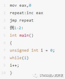
Example 1-2:
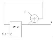
As can be seen, the above two examples both produce a continuously increasing sequence from 0, and both examples will continue to add until overflow and then start again from 0 (this depends on the word length of the computer, which is the number of bits of the CPU; eax is a 32-bit register, so it will inevitably add up to 4294967295 and then return to 0; the latter example depends on the type of adder and the number of D flip-flops used).
Then the question arises: what if I want a decreasing sequence? The first two examples are easy to explain; I can just change the code:
Example 2-1:
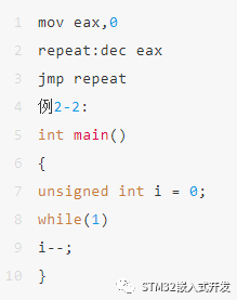
You just need to tap the keyboard lightly, and after modifying the code, it will execute as you wish.
But what about the latter example? You may have already thought of a solution: as shown in Example 2-2.
Example 2-2:
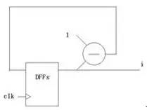
The problem arises; you cannot change the actual circuit by just tapping the keyboard! The above (Example 1-2) is an adder, but here it has turned into a subtractor (Example 2-2)!
In this case, you would need to make another circuit: one for addition and one for subtraction. But having two circuits means you need more circuits and chips, which will cost you more money. If you cannot use both circuits simultaneously, you would have spent twice as much money to do just one task! Related articles: How does a CPU perform digital addition?
Can this problem be solved? The answer is yes!
Example 2-3:
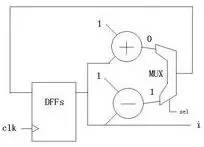
This example uses one adder and one subtractor, which does not save more than the previous circuit (obviously… do you expect to use a subtractor as an adder? Impossible! Of course, adding a negative number’s complement is indeed subtracting a number, but let’s not consider this issue for now).
Overall, the advantage is still evident (the difference between two circuit boards and one circuit board).
The sel signal is used for selection (0 for increasing, 1 for decreasing). If we consider the sel signal as the “program,” this circuit acts like a “CPU” that can execute different “operations” based on the “program.” Thus, through the “program” (sel signal), this circuit can achieve reuse.
Based on the above conclusion, I believe (this is just my personal opinion): the program is an extension of the hardware circuit!
And I believe that the basic idea of a CPU is just like this.
Next, we will analyze the structure of the CPU and its components, and then implement this CPU.
What is a single-cycle CPU, what is a multi-cycle CPU, what is RISC, what is CISC?
First, everyone should have a concept of a clock: this is a difficult problem to explain… It can be understood as the mechanical clock in your home, which ticks after you put in the battery, and its “tick” speed is the frequency, while the time taken for one tick is the period. Human activities, such as work, meals, and entertainment, are all conducted according to the clock’s indication (excluding night owls). Generally speaking, clock signals are produced by crystal oscillators, alternating signals of 0101 (low and high levels).
Digital circuits require a “clock” to drive them, just like a conductor is needed to lead a symphony; everyone follows the conductor’s beat to play, just as all components in a digital circuit work according to the clock’s rhythm.
The following is an ideal clock signal (note that this is ideal).
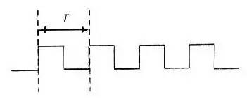
Of course, actual clock signals may not be so ideal; the rising edge may be sloped, the duty cycle may not be 50%, there may be jitter, and there may be offsets (relative to two devices), which can be distorted due to parasitic capacitance effects in the wires.
If you didn’t understand the previous section, that’s okay~~~ It just tells you that actual clock signals measured will definitely not be so standard.
The CPU’s operating frequency is the product of the external frequency and the multiplier (how the CPU calculates frequency, I’m not very clear about that either, haha). The CPU generates a clock signal through an external crystal oscillator and then multiplies it to the required frequency through internal circuits (phase-locked loop). Of course, someone might ask, why go through such trouble? Why not just make a clock crystal oscillator outside the circuit that can generate such a high clock signal? This is possible, and in some simple systems (like the 51 microcontroller), it is done this way. However, the CPU in a computing device is relatively complex; for some reasons, it must be done within the CPU.
Next, let’s briefly discuss the two instruction sets of CPUs: CISC and RISC.
Let me share my views (personal views; if there are mistakes, please correct me):
RISC stands for Reduced Instruction Set Computer, with a typical example being the MIPS processor.
CISC stands for Complex Instruction Set Computer, with a typical example being the x86 series processors (although the x86 instructions still resemble the original CISC instructions, the actual structure of the processors has transformed into a RISC structure, as RISC structures are easier to implement features like pipelining. If you are using an Intel processor from a certain series, it looks like it is using CISC instructions, but in reality, your CPU’s structure is already RISC).
Generally, CISC processors require microinstructions to operate in conjunction, while RISC is entirely implemented through hard wiring. This means that when a CISC processor executes your program, it must first read some data from another ROM to “guide” the processor on how to process your commands, which results in lower efficiency. In contrast, RISC achieves certain functions entirely through the connections between components, greatly enhancing work efficiency and providing a foundation for the emergence of pipelined structures. CISC processors have fewer registers, and instructions can implement some special functions, such as some registers in the 8086:
ax, bx, cx, dx, si, di, etc.; segment registers include: cs, ds, es, ss, etc. In contrast, the functions of RISC instructions are slightly weaker; for example:
To illustrate with the Nios embedded processor, the Nios processor has 32 general-purpose registers (r0~r31), while the functional capabilities of the instructions are relatively weaker than those of x86. Moreover, x86 performs memory access directly using the mov instruction, while the Nios processor uses load for reading memory and store for writing memory.
The ways they respond to interrupts are also different. For example, the x86 processor places the interrupt vector table at the lowest memory address (0-1023, with each interrupt vector occupying four bytes), accommodating 256 interrupts (taking the real mode of the 8086 as an example). When responding to an interrupt, it loads the cs and ip values from the address corresponding to the interrupt number into the cs and ip registers, saving the original address and the status register before entering interrupt handling. In contrast, RISC has a common interrupt response function, which finds the address of the function registered with the system according to the interrupt number and calls that function. Generally, the length of CISC instructions is variable, for example, x86’s xor ax, bx corresponds to machine code 0x31d8, while push ax is 0x50, and pop cx is 0x59. In contrast, RISC instructions are fixed-length, for example, 32 bits.
Related articles recommended: How does a CPU recognize the code we write? If there are still unclear points… feel free to search online; it takes some time to understand these concepts.
The basic structure of a CPU and necessary components
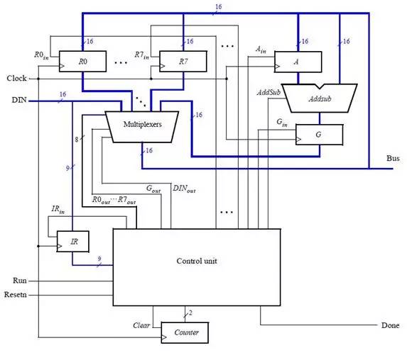
This example is cited from Lab Exercise 9 on the CD included with the DE2 development board kit. From the diagram, we can see that a CPU includes a set of general-purpose registers R0~R7, an ALU (Arithmetic Logic Unit), an instruction register IR, a controller (generally this part is a finite state machine or implemented with microinstructions), and the data path (the connections in the diagram). Of course, a real CPU cannot just contain these few components; this is a model CPU, meaning it only illustrates the principles of a CPU. A truly complex CPU involves many intricate structures and timing, such as using special registers in virtual mode, page table registers for supporting paging, TLB for speeding up memory access, and data cache and instruction cache for accelerating data and instruction access, etc. However, those are considerations for later; let’s start from this simple part.
The example can implement the following instructions:
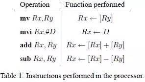
The mv instruction transfers data from Ry to Rx, while mvi transfers an immediate value D into Rx. The add instruction places the sum of Rx and Ry into Rx, and sub does the same but performs subtraction.
First, let’s explain how the mv instruction is executed: the mv instruction moves the value of Ry into the Rx register. Both registers consist of a set of D flip-flops, and the number of D flip-flops depends on the width of the register, such as 32-bit or 64-bit machines, meaning they use a different number of D flip-flops. When executing mv rx, ry, the multiplexer in the middle (the largest one in the diagram) selects Ry, allowing the Ry register to drive the bus. At this point, the signal on the Bus is the value of Ry; then, R0~R7 each have R0in~R7in signals, which are enable signals. When this signal is active, on the rising edge, the trigger will input the din data. Therefore, at this point, you must have thought that the Din signal on the Rx trigger will become active, and after one clock cycle, the value of Ry will be sent to Rx.
Similar to the mv instruction, the mvi instruction also sends data into Rx, except this time the data is stored in the instruction itself, which is the immediate value, so the Din signal of Rx will become active, and the multiplexer will select the data from IR because the immediate number exists in the instruction. It also undergoes certain processing, such as extension, etc.
The add instruction will first let the multiplexer select Rx, and then the Ain signal becomes active, so after one clock cycle, the data of Rx is sent into the A register of the ALU. At this time, the multiplexer selects Ry, and the addsub signal is set to add to indicate the ALU to perform addition. The Gin signal becomes active to store the calculation result in the G register, and after another clock cycle, the data in G will be the sum of Rx and Ry. At this point, the multiplexer selects Gin, and the Din signal of Rx becomes active; after one clock cycle, the data is stored in Rx.
The process of sub is similar to add, but the addsub signal is set to sub to indicate the ALU to perform subtraction.
This is the CPU model I created
Below, I will share the RTL netlist of the CPU model I created. I will upload the code, but this can only be simulated because there were issues with the design concept, leading to asynchronous designs and errors where the output of the state machine served as the clock input for another device. Therefore, this model can only be used for simulation. I used Synplify Pro to synthesize the RTL, and the state transition diagram was captured using Quartus’s FSM Viewer.
First, here is an overview of the entire system:
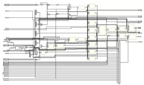
This is much more complex than the simple model above! But don’t worry, this is just a slightly more complex version of the CPU above. The difference is that this CPU is a multi-cycle CPU while the Lab Exercise above is a single-cycle CPU.
The following diagram shows the program counter (PC), which is commonly known as ip (instruction pointer) in x86 processors:
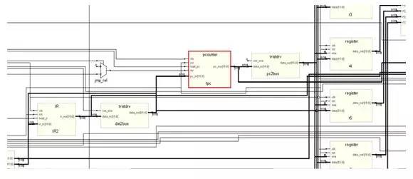
The red part is the PC, and behind it is a tri-state bridge, connected to the bus. The data here sometimes needs to be sent to the address bus for fetching data from memory to complete the Instruction Fetch process, and sometimes it needs to send the PC value to the data side of the general-purpose registers.
Next is the IR (Instruction Register), which is a typical feature of multi-cycle processors because the processor retrieves the machine code from memory in the first cycle and then stores it in this register. The subsequent states are executed based on the data in this register.
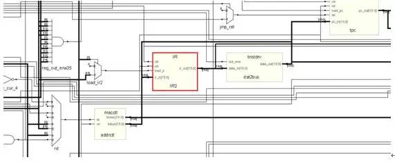
Next, let’s introduce the ALU, or Arithmetic Logic Unit, which performs arithmetic and logic operations. Typical arithmetic operations include:
For example: 1+1=2, 11×23=253, while typical logic operations include: 1 and 1=1, 0 or 0=0, 1<<3=8, which belongs to logical operations.
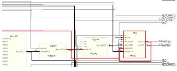 As can be seen from the diagram, the output of the ALU is connected to the back with a long wire. Referring to the entire CPU diagram, these wires connect to the general-purpose registers, allowing the results of calculations to be stored back. For example, when you use add eax,1, the value of eax is increased by 1 and then returned to eax. Thus, the ALU’s results need to be fed back to the general-purpose registers, and the ALU’s inputs should also come from the outputs of the general-purpose registers.
Next, let’s introduce ADDRMUX:
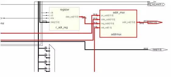
This component is used to select addresses. The output on the right is the CPU’s address bus, which has already been sent out of the CPU (i.e., you can see the pins on the chip’s exterior). The CPU’s address bus is sent to the address side of the memory. Modern computer systems are actually quite complex, so in reality, your computer’s CPU accesses memory through the Northbridge chip (of course, there are also cases where the memory controller is built into the CPU). The left side shows the sources of the addresses, which include general-purpose registers, the program counter, and also directly from the IR, as some immediate numbers contain memory address information.
Finally, let’s introduce the general-purpose registers:
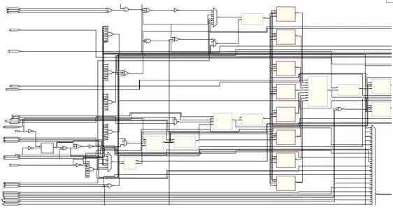 The purpose of general-purpose registers is to store intermediate values or to perform calculations. For example:add eax,2.
This is equivalent to eax+2, and then sent back to eax.
Lastly, let’s introduce the state machine, which is the “soul” of the CPU. If the components above give the CPU a “body,” then this part is the “soul” of the CPU:
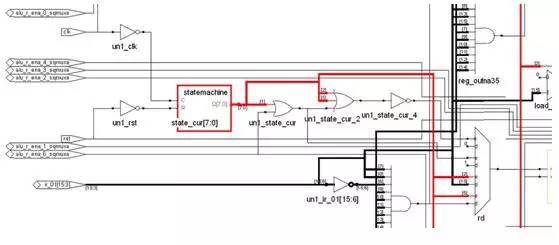 The state machine is connected to all components of the system, as all actions mentioned earlier require control from the state machine. The state machine is essentially composed of a memory circuit made up of flip-flops and a combinational logic part that serves as the next state decoding circuit, along with a part that decodes based on the current state and inputs to control various components. Below is a typical FSM structure from textbooks:
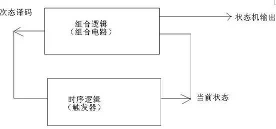
The state transition diagram we use is as follows:
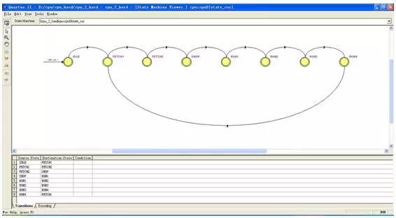 Since this processor design is very simple, there are not many states. After the processor goes through the above states, it completes executing an instruction.
Some CISC processors use microinstructions for control, which is similar to the role of the state machine. This structure appears in some older processors because the design tools and methods at that time were not as advanced as today, making hardware changes difficult and costly. Therefore, using microinstructions allowed for changes by simply modifying the microinstructions without needing to alter the hardware structure. Nowadays, electronic technology is highly developed, and design tools are comprehensive, so many processors are implemented directly through hard wiring.
With a good processor, we need to equip it with a good program. Next, we will use our designed processor to calculate the sum from 1 to 100. Since we have not designed a compiler or assembler, the program can only be written in machine code. The example program is as follows:
Let’s first write the assembly code for the program:
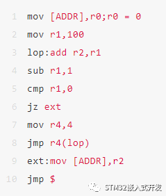
First, clear the address where data is stored in memory so that it can hold the results to be sent later. Then store the loop count (which is the upper limit for the sum) in the r1 register. Next, we will add the value of r1 to r2, where r2 is actually the register for holding the sum, and finally, we will send the value of r2 to a certain address in memory for storage.
Then subtract 1 from r1 and check if it is 0. If it is 0, it means the summation is complete; if not, it indicates that we need to continue. After completion, the program jumps to the ext part to store the result in a certain address in memory (the example given is 49152, which is binary 1100000000000000b). Finally, jmp $ is used to stop the program at this line, preventing it from running away (a runaway program can be very harmful! It may treat data as code or code as data!).
Converted to Verilog HDL language as follows:
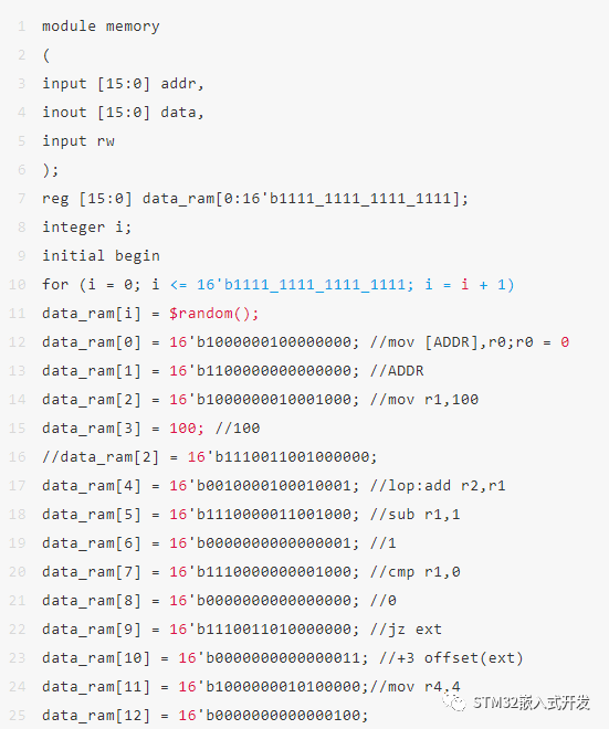
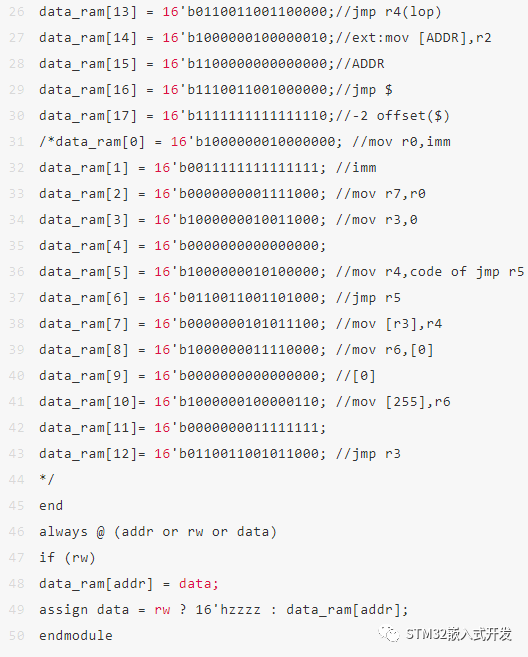
For the design, the CPU also requires a memory device (Memory). I modeled it using HDL, initializing each memory address with random data, and only a series of addresses starting from 0 were initialized with the code I wrote. The machine code corresponding to the assembly instructions has been given in the comments.
Then the result should be that r2 changes from 0 to 5050 (1+2+3+…+100=5050).
Meanwhile, r1 changes from 100 to 0, and once it reaches 0, the program will enter an infinite loop, stopping at jmp $. This is the beginning of the simulation:
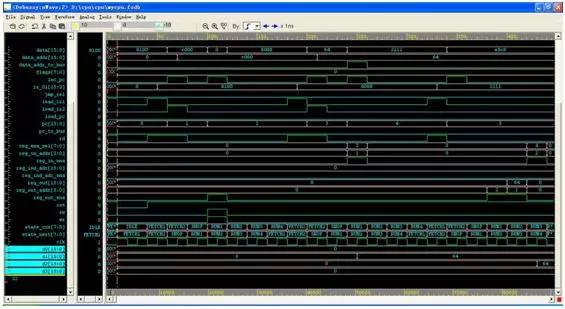 As you can see, after initialization, d0~d7 all become 0, which are the Q ends of registers r0~r7, and state_current and state_next are the current and next states of the state machine, respectively. All components of the CPU are controlled by this state machine, and the order of state names appearing corresponds to the order of connections in the FSM Viewer above.
Moreover, you can see that d2 changed to 0x64, which is decimal 100, indicating that the first addition has been executed.
Let’s take a look at the simulation results:
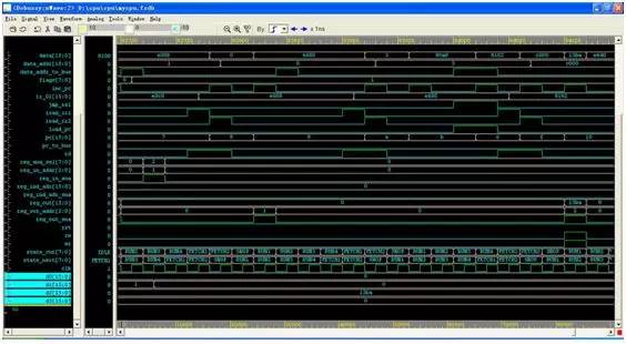 At this point, d1 has changed to 0 while d2 has changed to 0x13ba (decimal 5050), indicating that the program has successfully run within our designed processor and produced the result!
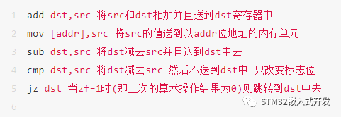
Lastly, here are some instructions I used (similar to x86):
Finally, let me mention that I synthesized the circuit using Synplify and simulated it with Debussy + ModelSim. Related materials can be referenced from: CPU Logic Design, by Zhu Ziyu and Li Yamin. Lab Exercise 9 is from the DE2 development disc.
The article is adapted from: STM32 Embedded Development(End)
More exciting content:
Yan Shi│Thoughts and Suggestions on the “Predicament” of Young Teachers in Colleges
Academician Zheng Weimin: Why Computer Majors Have Become Popular Choices for Examinees
【Directory】”Computer Education” 2022 Issue 6
【Directory】”Computer Education” 2022 Issue 5
【Directory】”Computer Education” 2022 Issue 4
【Directory】”Computer Education” 2022 Issue 3
【Directory】”Computer Education” 2022 Issue 2
【Directory】”Computer Education” 2022 Issue 1
【Editorial Board’s Message】Professor Li Xiaoming from Peking University: Reflections on the “Year of Classroom Teaching Improvement”…
Professor Chen Daoxu from Nanjing University: Teaching students to ask questions and teaching students to answer questions, which is more important?
【Yan Shi Series】: Trends in Computer Discipline Development and Their Impact on Computer Education
Professor Li Xiaoming from Peking University: From Fun Mathematics to Fun Algorithms to Fun Programming—A Path for Non-specialist Learners to Experience Computational Thinking?
Reflections on Several Issues in Building a First-class Computer Discipline
Professor Liu Yunhao from Tsinghua University Answers 2000 Questions About AI
Professor Zhan Dechen from Harbin Institute of Technology: A New Model to Ensure Teaching Quality in Colleges—Synchronous and Asynchronous Blended Teaching
【Principal Interview】Accelerating the Promotion of Computer Science Education—Interview with Professor Zhou Aoying, Vice President of East China Normal University
New Engineering and Big Data Major Construction
Learning from Others—Compilation of Research Articles on Computer Education at Home and Abroad