Click the blue text

Follow us

In the electronics market of Huaqiangbei, Shenzhen, a 7-nanometer chip the size of a fingernail is priced at 300 yuan, while the cost of SMIC’s 14-nanometer chip has dropped to 150 yuan. Behind this price inversion is the survival logic of China’s chip manufacturing industry amid technological gaps and global competition. When the U.S. Department of Commerce announced export restrictions on NVIDIA’s H20 chip on April 15, Huawei’s Ascend 920 was accelerating mass production, utilizing SMIC’s 6-nanometer process, achieving 83% of H20’s performance. This “silicon-based war” concerning industrial security is reshaping the global semiconductor landscape.
(Image from the internet)
1. The “Dual Mirror” of Manufacturing Capability: The King of Mature Processes and the Predicament of Advanced Processes
1. The “Chinese Advantage” in Mature Processes
SMIC’s 14-nanometer process yield has improved to 85%, with a monthly production capacity exceeding 15,000 wafers, covering fields such as the Internet of Things and consumer electronics. Its 28-nanometer production line is operating at full capacity, supporting the core demands of domestic 5G base stations and automotive electronics. Yangtze Memory’s 232-layer 3D NAND flash memory is produced using domestic equipment, and although the number of layers is 70 fewer than earlier products, through process optimization, the storage density still reaches international mainstream levels. Hefei Changxin’s 19-nanometer DRAM chips have achieved mass production, filling a domestic gap.
This breakthrough in mature processes is essentially a concentrated release of the “engineer dividend” of China’s manufacturing industry. Huahai Qingshi’s CMP equipment has processed over 1.2 million wafers, with yields at an internationally leading level; North Huachuang’s 5-nanometer etching machine has entered the international supply chain, with a market share exceeding 15%. These devices not only reduce the cost of domestic chip manufacturing but also build a complete industrial chain from design to packaging and testing.
2. The “Bottleneck” Dilemma of Advanced Processes
In processes of 7 nanometers and below, China still faces dual challenges of physical limits and equipment blockades. SMIC’s 7-nanometer R&D relies on DUV multiple exposure technology, which can achieve equivalent 7-nanometer processes but has 30% higher power consumption than EUV lithography, and the mass production yield is below 50%. Shanghai Micro Electronics’ 28-nanometer lithography machine has entered the testing phase, but its key optical components still rely on imports, making the 2025 mass production timeline uncertain.
The bottleneck in materials is also significant. The localization rate of key materials such as photoresists and high-purity silicon wafers is less than 20%, and SMIC’s 14-nanometer process still requires imported JSR products from Japan for photoresists. This “equipment – materials – process” collaborative shortcoming makes breakthroughs in advanced processes extremely difficult for China.
(Image from the internet)
2. The “Four Battlefields” of Technical Challenges
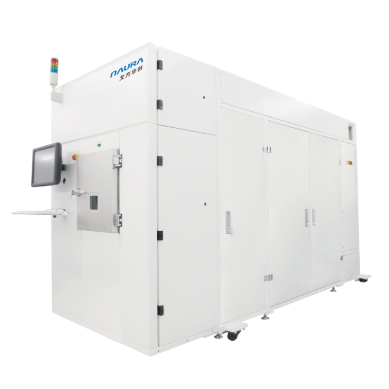
1. Lithography Machines: From Dependence on ASML to Domestic Substitution
ASML’s EUV lithography machines are fully restricted from export to China, and the maintenance and upgrades of DUV lithography machines are also facing restrictions from the Dutch government. This blockade has forced the acceleration of domestic substitution: Shanghai Micro Electronics’ SSA800 lithography machine uses a 193-nanometer ArF light source and achieves 28-nanometer processes through multiple exposures, with wafer non-uniformity controlled within 3%. Although its efficiency is only 60% of ASML’s similar products, it has already achieved small batch verification at SMIC and Hua Hong Semiconductor.
2. EDA Tools: From Ecological Deficiency to Partial Breakthroughs
The domestic substitution in the EDA field is shifting from “single-point breakthroughs” to “system reconstruction”. Huada Empyrean’s full-process tools for analog circuit design have passed Samsung’s 14-nanometer certification, and its physical verification tools support 28-nanometer processes; Geken Electronics’ device modeling and circuit simulation tools have replaced Synopsys products in memory chip design. In 2023, domestic EDA’s global market share increased to 3%, reaching 20% in the domestic market, but for processes below 7 nanometers, it still relies on Synopsys and Cadence’s toolchains.
3. Third-Generation Semiconductors: From Laboratory to Industrialization
Silicon carbide (SiC) and gallium nitride (GaN) have become the “second battlefield” of China’s semiconductor industry. Innoscience’s 8-inch silicon-based GaN production line has achieved large-scale applications, with revenue growth of nearly 40% in 2024; Hunan Sanan’s silicon carbide MOSFET chips have been used in BYD’s 800V high-voltage platform, enhancing electric vehicle range by 5%-10%. Beijing’s lattice field’s liquid-phase silicon carbide substrate technology has reduced chip costs by 30%, supporting the demand for photovoltaic inverters and smart grids.
4. Talent Competition: From Global Poaching to Local Cultivation
In response to the talent siphoning of the U.S. CHIPS and Science Act, China has launched a “Global Semiconductor Talent Recruitment Program”. SMIC has poached 195 engineers from TSMC, and Huawei HiSilicon has established an R&D center in Munich, Germany, to attract European talent. Domestic universities are expanding the enrollment scale of microelectronics majors by three times through the “industry-education joint system”, and the “chip engineers” jointly trained by Tsinghua University and SMIC have entered production lines.
(Image from the internet)
3. The “Dual Circulation” Reconstruction of the Industrial Ecosystem
1. Policy Toolbox: From Financial Support to Ecological Construction
The National Big Fund Phase III, with 344 billion yuan, focuses on semiconductor manufacturing and equipment materials, with a $20 billion investment from Middle Eastern sovereign funds into SMIC, and Saudi Arabia launching the “Red Sea Chip Corridor” plan. Local governments’ “policy combinations” are more targeted: Shenzhen provides a 70% subsidy for companies purchasing domestic EDA tools, and Shanghai offers up to 100 million yuan in R&D funding for third-generation semiconductor projects.
2. Market Breakthrough: From Domestic Substitution to Global Competition
In the analog chip field, products from Shengbang Co. and Fuman Micro are still profitable at prices 20% lower than American competitors; Aiwei Electronics’ high-performance mixed-signal chips are expected to exceed 6 billion units in sales in 2024. This cost advantage is reshaping the global supply chain: Texas Instruments’ $3 billion sales in China will see about 20% of profits swallowed by a 125% tariff; Intel may be forced to exit the Chinese market if it insists on local wafer production.
3. Technical Challenges: From Following to Leading
In 2024, Zhongwei’s CCP etching equipment will produce over 1,200 reaction chambers, with a cumulative installed capacity exceeding 4,000 reaction chambers; Shanghai Jingce Electronics has achieved the localization of 12-inch wafer full-process testing equipment. In the advanced packaging field, Changdian Technology’s 3D packaging technology has achieved line widths below 10μm, with HBM orders accounting for 40%.
(Image from the internet)
4. The Next Decade: The “Silicon-Based Long March” of New Productive Forces
1. Technical Trends: Deep Integration of AI and Semiconductors
The intelligent upgrade of humanoid robots will spur explosive demand for AI chips. According to predictions from the China Electronics Society, by 2030, the market size for humanoid robots in China will exceed 870 billion yuan, driving semiconductor demand growth of over 300 billion yuan. Chipone Semiconductor’s AI cockpit chip supports integrated docking functions, and Yiswei’s autonomous driving chip has entered the supply chain of automotive companies, while Beijing’s humanoid robot innovation center accelerates the collaborative R&D of chips and algorithms.
2. Industrial Synergy: The “Chip” Ecosystem of Beijing-Tianjin-Hebei
The coordinated development strategy of Beijing-Tianjin-Hebei injects new momentum into the semiconductor industry. Tianjin Huahai Qingshi’s CMP equipment, Shijiazhuang Zhongdian’s third-generation semiconductor materials, and Baoding’s packaging and testing base jointly construct a complete industrial chain of “design – manufacturing – packaging and testing”. This regional synergy not only reduces enterprise costs but also accelerates innovation iteration through technology sharing.
3. Policy Outlook: Cultivating New Productive Forces
Beijing’s “14th Five-Year Plan” clearly lists semiconductors as a strategic emerging industry, planning to build the largest domestic integrated circuit production capacity and the strongest technological innovation capability by 2025. Yizhuang, as a core bearing area, is attracting international resources through the “Unicorn Enterprise Global Network Link Action”, promoting companies like Chipone Semiconductor and Landspace Aerospace to form new productive forces in AI and commercial aerospace.
(Image from the internet)
Conclusion

From the chip counters in Huaqiangbei to the clean rooms of SMIC, China’s chip manufacturing industry is undergoing an “extreme challenge”. While the U.S. attempts to build walls with tariffs, Chinese companies are opening new tracks with technological breakthroughs and ecological reconstruction at the Canton Fair. As Professor Zhou Peng of Fudan University stated: “Two-dimensional semiconductors will complement silicon-based chips for a long time, but the former will dominate disruptive innovation in the next decade.” This “silicon-based long march” concerning technological sovereignty and industrial security not only determines the ownership of the trillion-level smart car market but will also redefine the rules of global technological competition.

END
Previous Highlights

China’s Semiconductor “Origin” New Regulations: Breaking the Deadlock Under Strategic Game
Tariff Strangulation and Industrial Reconstruction: China’s Semiconductor Breakthrough Moment
Chip Manufacturing Process—Wafer Manufacturing 1
The Development History of Chip Manufacturing Process: From Vacuum Tubes to AI Chips
Disclaimer
This article’s content is sourced from the internet and published materials, and we maintain neutrality regarding the views expressed in the article, which are for readers’ reference and discussion only. The copyright of the reproduced articles belongs to the original authors and publishing institutions. If there is any infringement, please contact us for deletion. We welcome readers to contact the editorial team through the backend for submissions, recommendations, suggestions, or discussions on cooperation opportunities. Thank you all for your attention and support!
Contact Us
Public account email: [email protected]