How Image Sensors Drive the Development of Embedded Vision Technology

How Image Sensors Drive the Development of Embedded Vision Technology

New imaging applications are flourishing, from collaborative robots in Industry 4.0, to drones for firefighting or agriculture, to biometric facial recognition, and handheld medical devices for home care. A key factor behind the emergence of these new application scenarios is that embedded vision is more prevalent than ever. Embedded vision is not a new concept; it simply defines a system that includes a vision setup that controls and processes data without an external computer. It has been widely used in industrial quality control, with the most familiar example being the “smart camera.”

In recent years, the development of affordable hardware components from the consumer market has significantly reduced the bill of materials (BOM) costs and product size compared to previous computer-based solutions. For example, small system integrators (OEMs) can now source single-board computers or module systems like NVIDIA Jetson in small batches; larger OEMs can directly obtain image signal processors like Qualcomm Snapdragon. On the software side, available software libraries can accelerate the development speed of dedicated vision systems and reduce configuration difficulties, even for small batch production.

The second change driving the development of embedded vision systems is the emergence of machine learning, which enables neural networks in laboratories to be trained and then uploaded directly to processors so that they can automatically recognize features and make decisions in real-time.

Providing solutions suitable for embedded vision systems is crucial for imaging companies targeting these high-growth applications. Image sensors play an important role in large-scale adoption as they directly influence the performance and design of embedded vision systems, and their main driving factors can be summarized as: smaller size, weight, power consumption, and cost, abbreviated in English as “SWaP-C” (decreasing Size, Weight, Power, and Cost).

1

Reducing costs is crucial

The accelerators for new applications of embedded vision are the prices that meet market demand, and the cost of vision systems is a major constraint to achieving this requirement.

1

Saving optical costs

The first way to reduce the cost of vision modules is to shrink product size, for two reasons: first, the smaller the pixel size of the image sensor, the more chips can be manufactured from a wafer; on the other hand, sensors can use smaller and lower-cost optical components, both of which can reduce inherent costs. For example, Teledyne e2v’s Emerald 5M sensor reduces pixel size to 2.8µm, allowing S-mount (M12) lenses to be used on five-megapixel global shutter sensors, resulting in direct cost savings—the entry-level M12 lens costs about $10, while larger C-mount or F-mount lenses cost 10 to 20 times more. Therefore, reducing size is an effective way to lower the cost of embedded vision systems.
For image sensor manufacturers, this reduced optical cost has another impact on design, as generally, the lower the optical cost, the less ideal the angle of incidence for the sensor. Therefore, low-cost optics require specific displacement microlenses to be designed above the pixels to compensate for distortion and focus light from wide angles.

2

Cost-effective sensor interfaces

In addition to optical optimization, the choice of sensor interface also indirectly affects the cost of vision systems. The MIPI CSI-2 interface is the most suitable choice for achieving cost savings (it was originally developed by the MIPI Alliance for the mobile industry). It has been widely adopted by most ISPs and is starting to be used in the industrial market because it provides a lightweight integration from low-cost system-on-chip (SoC) or system-on-module (SoM) from NXP, NVIDIA, Qualcomm, Rockchip, Intel, and others. Designing a CMOS image sensor with a MIPI CSI-2 sensor interface allows data from the image sensor to be transmitted directly to the host SoC or SoM of the embedded system without any adapter bridges, thus saving costs and PCB space, especially in multi-sensor-based embedded systems (like 360-degree panoramic systems).
However, these benefits are limited by some constraints. The MIPI CSI-2 D-PHY standard widely used in the machine vision industry relies on cost-effective flat ribbon cables, which have the drawback of limiting connection distances to 20 centimeters, which may not be optimal for remote pan-tilt setups where the sensor is far from the main processor, often seen in traffic monitoring or surround view applications. One solution for extending connection distances is to place additional repeater boards between the MIPI sensor board and the host processor, but this comes at the cost of miniaturization. Other solutions come not from the mobile industry but from the automotive industry: the so-called FPD-Link III and MIPI CSI-2 A-PHY standards support coaxial or differential pairs, allowing connection distances of up to 15 meters.

3

Reducing development costs

When investing in new products, the rising development costs are often a challenge, which can incur millions of dollars in one-time non-recurring engineering (NRE) costs and pressure time to market. For embedded vision, this pressure is even greater, as modularity (i.e., whether a product can switch between multiple image sensors) is an important consideration for integrators. Fortunately, one-time development costs can be controlled by providing a certain degree of cross-compatibility between sensors, for example, by defining merged/shared pixel structures for stable photoelectric performance, sharing a single frontend structure through the same optical center, and compatible PCB components (by size compatibility or pin compatibility), thus speeding up evaluation, integration, and supply chain, as shown in Figure 1.
How Image Sensors Drive the Development of Embedded Vision Technology
Figure 1: Image sensor platforms can be designed for pin compatibility (left) or size compatibility (right) for proprietary PCB layout designs.
Today, with the widespread release of so-called modular and board-level solutions, the development speed of embedded vision systems is faster and more affordable. These one-stop products usually include a sensor board that can be integrated at any time, sometimes also including a preprocessing chip, a mechanical front, and/or a lens interface. These solutions bring benefits through highly optimized sizes and standardized connectors, allowing direct connection to off-the-shelf processing boards like NVIDIA Jetson or NXP i.MX ones without the need to design or manufacture intermediate adapter boards. By eliminating the need for PCB design and manufacturing, these module or board-level solutions not only simplify and accelerate hardware development but also significantly shorten software development time, as they are often provided with Video4Linux drivers.
Thus, original equipment manufacturers and vision system manufacturers can skip weeks of development time to make image sensors communicate with the main processor, allowing them to focus on their distinctive software and overall system design. Optical modules, such as those provided by Teledyne e2v, which integrate the lens within the module, offer a complete package from optics to driver to sensor board, further promoting the development of one-stop solutions.
How Image Sensors Drive the Development of Embedded Vision Technology
Figure 2: New modules (right) allow direct connection to off-the-shelf processing boards (left) without designing any other adapter boards.

2

Improving autonomous energy efficiency

Due to external computers hindering portable applications, battery-powered devices are the most obvious application benefiting from embedded vision. To reduce the system’s energy consumption, image sensors now include multiple functions that allow system designers to save energy.
From the perspective of sensors, there are several ways to reduce the power consumption of vision systems without decreasing the acquisition frame rate. The simplest method is to minimize the dynamic operation of the sensor itself at the system level by using standby or idle mode for as long as possible, thus reducing the power consumption of the sensor itself. Standby mode reduces the power consumption of the sensor to below 10% of working mode by turning off simulation circuits. Idle mode can halve power consumption and allows the sensor to restart and capture images in a matter of microseconds.
Another energy-saving method is to use more advanced lithography node technologies to design sensors. The smaller the technology node, the lower the voltage required to switch transistors, thus reducing dynamic power consumption, as power consumption is proportional to the square of the voltage. Therefore, pixels produced with 180nm technology ten years ago not only reduced the size of transistors to 110nm but also reduced the voltage of digital circuits from 1.8V to 1.2V. The next generation of sensors will use 65nm technology nodes, making embedded vision applications more energy-efficient.
Finally, by selecting the appropriate image sensor, it is possible to reduce the energy consumption of LED lights under certain conditions. Some systems must use active illumination, such as generating three-dimensional maps, motion pauses, or simply using sequential pulses of specified wavelengths to enhance contrast. In these cases, reducing the noise of the image sensor in low-light environments can achieve lower power consumption. By reducing sensor noise, engineers can determine whether to reduce current intensity or the number of LED lights integrated into the embedded vision system. In other cases, when image capture and LED flashing are triggered by external events, selecting the appropriate sensor readout structure can significantly save energy. When using traditional rolling shutter sensors, the LED lights must be fully on during the entire exposure of the frame, while global shutter sensors allow LEDs to be turned on only in parts of the frame. Therefore, when using pixel-wise correlated double sampling (CDS), replacing rolling shutter sensors with global shutter sensors can save lighting costs while still maintaining noise levels as low as those seen with CCD sensors used in microscopes.

3

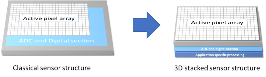
On-chip functions pave the way for programming vision systems

Some expanded concepts of embedded vision lead us to fully customize image sensors to integrate all processing functions (system-on-chip) in a 3D stacked manner for optimized performance and power consumption. However, the cost of developing such products is very high, and achieving this level of integration with fully customized sensors is not entirely impossible in the long run, but we are currently in a transitional phase, incorporating certain functions directly into the sensor to reduce computational load and speed up processing time.
For example, in barcode reading applications, Teledyne e2v has patented technology that incorporates an embedded function with a proprietary barcode recognition algorithm into the sensor chip, which can identify the location of barcodes within each frame, allowing the image signal processor to focus only on these areas, improving data processing efficiency.
How Image Sensors Drive the Development of Embedded Vision Technology
Figure 3. Teledyne e2v Snappy five-megapixel chip automatically identifies barcode locations.
Another function that reduces processing load and optimizes “good” data is Teledyne E2V’s patented fast exposure mode, which enables the sensor to automatically correct exposure times to avoid saturation under changing lighting conditions. This feature optimizes processing time as it adapts to fluctuations in lighting within a single frame, and this quick response maximizes the number of “bad” images that the processor needs to handle.
These functions are often specific and require a good understanding of customer applications. As long as there is sufficient understanding of the application, various other on-chip functions can be designed to optimize embedded vision systems.

4

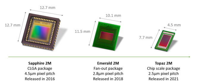
Reducing weight and size to fit minimal application spaces

Another major requirement for embedded vision systems is the ability to fit into tight spaces or be lightweight for handheld devices or to extend battery-powered product working times. This is why most embedded vision systems now use low-resolution small optical format sensors ranging from 1MP to 5MP.
Reducing the size of pixel chips is just the first step in reducing the size and weight of image sensor packages. The current 65nm process allows us to reduce the global shutter pixel size to 2.5µm without sacrificing photoelectric performance. This production process enables full HD global shutter CMOS image sensors to meet the mobile market’s requirement of being less than 1/3 inch in size.
Another major technology for reducing sensor weight and footprint is shrinking package size. Wafer-level packaging has rapidly grown in the market over recent years, particularly evident in mobile, automotive, and medical applications. Compared to traditional ceramic (CLGA) packages commonly used in the industrial market, wafer-level fan-out packages and chip-scale packages can achieve higher density connections, making them excellent solutions for the lightweight and miniaturization challenges of embedded system image sensors. For Teledyne e2v’s two-megapixel sensor, wafer-level packaging combined with smaller pixel sizes has reduced the size to a quarter in just five years.
How Image Sensors Drive the Development of Embedded Vision Technology
Figure 4: Typical evolution of image sensor sizes due to packaging technology improvements and pixel size reductions since 2016.
Looking ahead, we anticipate that new technologies will further achieve smaller sensor sizes required for embedded vision systems.
3D stacking is an innovative technology for semiconductor device manufacturing, the principle of which is to manufacture various circuit chips on different wafers and then stack and interconnect them using copper-to-copper connections and Through Silicon Vias (TSV) technology. 3D stacking, being a multi-layer overlapping chip, allows devices to achieve smaller package sizes than traditional sensors. In 3D stacked image sensors, readout and processing blocks can be moved below the pixel array and row decoders. This reduces the footprint size of the sensor due to the smaller readout and processing blocks and allows for more processing resources to be added to reduce the load on the image signal processor.
How Image Sensors Drive the Development of Embedded Vision Technology
Figure 5: 3D chip stacking technology allows pixel arrays, simulation, and digital circuits to overlap, even adding extra specific application processing layers while reducing sensor area.
However, to make 3D stacking technology widely used in the image sensor market, there are still some challenges. First, this is an emerging technology; second, it is costly due to additional processing steps, making chip costs over three times higher than chips using traditional technologies. Therefore, 3D stacking will mainly be an option for high-performance or very small package size embedded vision systems.
In summary, embedded vision systems can be summarized as a “lightweight” vision technology that can be used by various types of companies, including OEMs, system integrators, and standard camera manufacturers. “Embedded” is a general description that can be used for different applications, thus cannot provide a list to describe its characteristics. However, there are several applicable principles for optimizing embedded vision systems: generally, market drivers do not come from super-fast speeds or ultra-high sensitivity, but rather from size, weight, power consumption, and cost. Image sensors are the main drivers of these conditions, so careful selection of suitable image sensors is needed to optimize the overall performance of embedded vision systems.
Suitable image sensors can provide more flexibility for embedded designers, not only saving BOM costs but also reducing the footprint of lighting and optical components. But more importantly than image sensors, the emergence of ready-to-use board-level solutions in the form of imaging modules paves the way for further optimization of size, weight, power consumption, and cost, significantly reducing development costs and time through cost-effective, deep-learning optimized image signal processors from the consumer market, without adding extra complexity.
Written by: Marie-Charlotte Leclerc
Source: Teledyne Imaging

This public account is a high-paying long-term column author. Welcome technology practitioners or enthusiasts with excellent writing skills to contact Sensor Editor: YG18511751369 (WeChat ID)

Looking forward to the next article with 100,000+ views from you!

Disclaimer: The copyright of this article belongs to the original author. If any videos, images, or text used in this article involve copyright issues, please notify us as soon as possible, and we will confirm copyright based on the proof materials you provide and pay remuneration according to national standards or delete the content immediately! The content of this article reflects the original author’s views and does not represent the views of this public account or bear responsibility for its authenticity.

How Image Sensors Drive the Development of Embedded Vision Technology

To publish your products, please click “Read the original text”

How Image Sensors Drive the Development of Embedded Vision Technology

Leave a Comment