Today, we will discuss the “level shifting” circuit below, which is quite enjoyable to understand. Circuit design can actually be very interesting.
First, let’s talk about the purpose of this circuit: when two MCUs operate at different working voltages (for example, MCU1 operates at 5V and MCU2 operates at 3.3V), how can MCU1 and MCU2 communicate via serial port?Related article:Example of Serial Communication between STM32 and 51 Microcontroller.It is clear that the corresponding TX and RX pins cannot be directly connected, as this may burn out the MCU with the lower operating voltage!
The following “bidirectional level shifting circuit” can achieve serial communication between MCUs with different VDD (chip operating voltages).
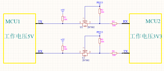
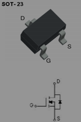
The core of this circuit lies in the MOS field-effect transistor (2N7002). It functions similarly to a transistor and can be used as a switch to control the circuit’s on and off states. However, compared to transistors, MOSFETs have many advantages, which will be discussed in detail later. Below is a 3D image and circuit diagram of the MOSFET. In simple terms, to use it as a switch, you only need to ensure that Vgs (the gate-source voltage) reaches a certain value, at which point the D and S pins will conduct; if Vgs does not reach this value, it will be off.
So how do we apply the 2N7002 in the above circuit, and what role does it play? Let’s analyze it below.
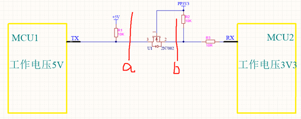
If we cut the circuit along lines a and b, then the TX pin of MCU1 is pulled up to 5V, and the RX pin of MCU2 is also pulled up to 3.3V. When the S and D pins of the 2N7002 (corresponding to pins 2 and 3 in the diagram) are off, it is equivalent to cutting the circuit along lines a and b. This means that when the 2N7002 is off, it can supply the corresponding operating voltage to the pins of both MCUs.
Next, let’s analyze:
Data transmission direction: MCU1 –> MCU2.
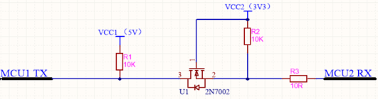
1. MCU1 TX sends a high level (5V), and MCU2 RX is configured as a serial port receiving pin. At this time, the S and D pins of the 2N7002 (corresponding to pins 2 and 3 in the diagram) are off, and the diode inside the 2N7002 does not conduct from 3 to 2. Therefore, MCU2 RX is pulled up to 3.3V by VCC2.
2. MCU1 TX sends a low level (0V), and the S and D pins of the 2N7002 remain off. However, the diode inside the 2N7002 conducts from 2 to 3, forming a loop with VCC2, R2, the diode in the 2N7002, and MCU1 TX. The pin 2 of the 2N7002 is pulled low, resulting in MCU2 RX being 0V. This circuit achieves level shifting from MCU1 to MCU2.
Next, let’s analyzeData transmission direction: MCU2 –> MCU1
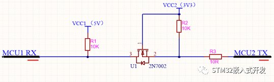
1. MCU2 TX sends a high level (3.3V), at this time, the Vgs (the voltage difference between pins 1 and 2 in the diagram) is approximately 0, and the 2N7002 is off. The diode inside the 2N7002 does not conduct from 3 to 2, and MCU1 RX pin is pulled up to 5V by VCC1.
2. MCU2 TX sends a low level (0V), at this time, the Vgs (the voltage difference between pins 1 and 2 in the diagram) is approximately 3.3V, and the 2N7002 conducts. The diode inside the 2N7002 does not conduct from 3 to 2, forming a loop with VCC1, R1, the diode in the 2N7002, and MCU2 TX. The pin 3 of the 2N7002 is pulled low, resulting in MCU1 RX being 0V.
This circuit achieves level shifting from MCU2 to MCU1.
Thus, we have completed the analysis of this circuit, which is a bidirectional serial level shifting circuit.
Advantages of MOSFETs:
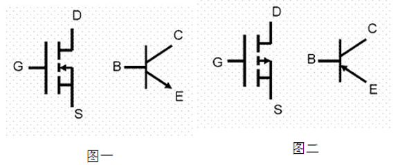
1. The source S, gate G, and drain D of the field-effect transistor correspond to the emitter e, base b, and collector c of a transistor, respectively. Their functions are similar. Figure 1 shows the pin configuration of an N-channel MOSFET and an NPN transistor, while Figure 2 shows the pin configuration of a P-channel MOSFET and a PNP transistor. Related article:MOSFET Basics.
2. Field-effect transistors are voltage-controlled current devices, controlled by VGS for ID, while ordinary bipolar transistors are current-controlled current devices, controlled by IB for IC. The transconductance (gm) of a MOSFET indicates how many amperes the drain current changes when the gate voltage changes by one volt. The current gain (beta β) of a bipolar transistor indicates how many collector current changes when the base current changes by one milliamp.3. The gate of a field-effect transistor is insulated from other electrodes, so it does not generate current; while the base current IB of a bipolar transistor determines the collector current IC. Therefore, the input resistance of a field-effect transistor is much higher than that of a bipolar transistor.4. Field-effect transistors conduct with only majority carriers; bipolar transistors conduct with both majority and minority carriers. Since the concentration of minority carriers is greatly affected by temperature and radiation, field-effect transistors have better temperature stability than bipolar transistors.5. When the source of a field-effect transistor is not connected to the substrate, the source and drain can be interchanged with little change in characteristics, while the characteristics of a bipolar transistor differ significantly when the collector and emitter are interchanged, resulting in a significant decrease in beta value.6. Field-effect transistors have a very low noise figure, making them suitable for the input stage of low-noise amplifiers and circuits requiring high signal-to-noise ratios.7. Both field-effect transistors and ordinary bipolar transistors can form various amplifier and switching circuits, but field-effect transistors have simpler manufacturing processes and possess excellent characteristics that ordinary bipolar transistors cannot match. They are gradually replacing ordinary bipolar transistors in various circuits and applications, and are widely used in large-scale and ultra-large-scale integrated circuits.8. High input impedance and low driving power: Since the gate-source insulation layer is made of silicon dioxide (SiO2), the DC resistance between the gate and source is essentially the insulation resistance of SiO2, which generally reaches around 100MΩ. The AC input impedance is mainly the capacitive reactance of the input capacitance. Due to the high input impedance, there is no voltage drop across the excitation signal, so it can be driven with very low power (high sensitivity). Ordinary bipolar transistors require a base voltage Vb to generate base current Ib, which in turn produces collector current. The driving power for bipolar transistors is required (Vb × Ib).9. Fast switching speed: The switching speed of MOSFETs is greatly related to their input capacitive characteristics. Due to the presence of input capacitive characteristics, the switching speed slows down. However, when used as a switch, reducing the driving circuit’s internal resistance can speed up the switching speed (using the “current sink circuit” described later to accelerate the charging and discharging time of the capacitance). MOSFETs rely solely on majority carrier conduction, without minority carrier storage effects, resulting in very rapid turn-off processes, with switching times between 10-100ns and operating frequencies exceeding 100kHz. Ordinary bipolar transistors, due to minority carrier storage effects, always exhibit hysteresis in switching, which affects the improvement of switching speed (currently, switching power supplies using MOSFETs can easily achieve operating frequencies of 100K/S to 150K/S, which is unimaginable for ordinary high-power bipolar transistors).10. No secondary breakdown: Ordinary power bipolar transistors exhibit a phenomenon where an increase in temperature leads to an increase in collector current (positive temperature-current characteristics), which further increases temperature, leading to a vicious cycle. The breakdown voltage VCEO of bipolar transistors decreases with increasing temperature, resulting in a continuous rise in temperature and a decrease in breakdown voltage, ultimately leading to breakdown. This is a destructive thermal breakdown phenomenon that accounts for 95% of the damage to TV switch power transistors and line output transistors, also known as secondary breakdown. MOSFETs exhibit the opposite temperature-current characteristics, where the channel current IDS decreases as the temperature (or ambient temperature) rises. For example, a MOSFET switch with IDS=10A at a control voltage VGS remains unchanged; at 25°C, IDS=3A, and at 100°C, IDS decreases to 2A. This negative temperature coefficient of channel current IDS prevents the occurrence of a vicious cycle and thermal breakdown. Therefore, using MOSFETs as switching devices significantly reduces the failure rate of switching devices. In recent years, the replacement of ordinary bipolar transistors with MOSFETs in TV switch power supplies has greatly reduced the failure rate of switching devices, which is a strong testament to this.11. The conduction characteristics of MOSFETs are purely resistive after they are turned on: Ordinary bipolar transistors have a very low voltage drop when saturated, known as saturation voltage drop. Since there is a voltage drop, the equivalent resistance of an ordinary bipolar transistor in saturation is a very small resistance, but this equivalent resistance is nonlinear (the voltage across the resistance and the current flowing through it do not comply with Ohm’s law). In contrast, when MOSFETs are used as switching devices, they also exhibit a very small equivalent resistance in saturation, but this resistance behaves like a linear resistance, where the resistance value and the voltage drop across it comply with Ohm’s law. When the current is large, the voltage drop is large; when the current is small, the voltage drop is small. Since the equivalent resistance is linear, linear components can be used in parallel. Therefore, when the power of one MOSFET is insufficient, multiple MOSFETs can be used in parallel without additional balancing measures (nonlinear devices cannot be directly used in parallel).