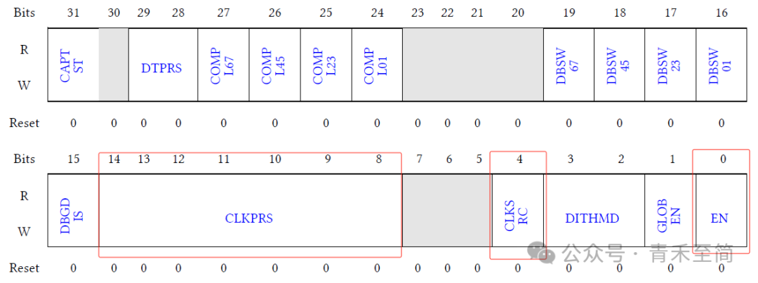
eTMR (Enhanced Timer) module supports general Timer, PWM generation, output comparison, input capture, QD quadrature decoding, and digital fractional division Dithering, mainly suitable for automotive applications such as motor control, lighting control, and power management. eTMR is comparable to NXP’s eFlexPWM and FTM.This article provides a detailed explanation of the principles of PWM generation, including the types of PWM generated: edge-aligned PWM, center-aligned PWM, asymmetric PWM, and windowed PWM types; the loading mechanism of shadow registers, etc. It is mainly applicable to automotive applications for motor control.Part 1. Basic Principles of PWM Generation1. Interpretation of Related Registers(1) Overall Control Register Fields of eTMR:
- CTRL[EN] is the global enable switch, generally configured last; after setting to ‘1’, the counter starts counting.
- CTRL[CLKSRC] is the clock selection:
- 0b – Module bus clock (default);
- 1b – External clock, which can come from a PIN or the functional clock of the IPC module.
- CTRL[CLKPRS] performs division based on the selected clock source, with the division value being (CTRL[CLKPRS]+1).
 (2) Counter Register Fields:
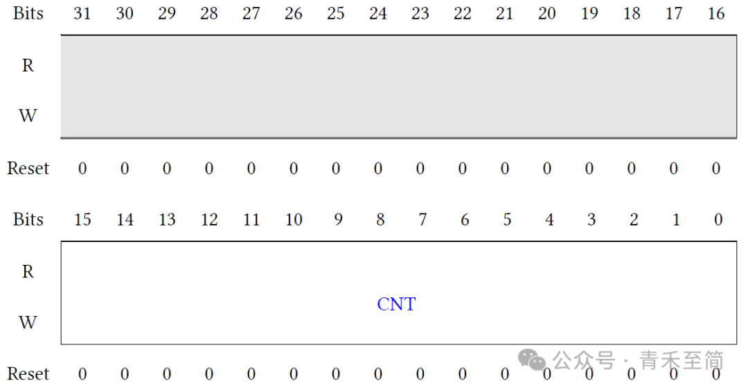
- CNT[CNT] supports read and write functions. When CTRL[EN]=0 and SYNC[CNTINIT]=0, writing to register CNT[CNT] can initialize the counter to the value of CNT[CNT]. After enabling the counter (i.e., after CTRL[EN]=1), the starting value of the first counting cycle begins from CNT[CNT].
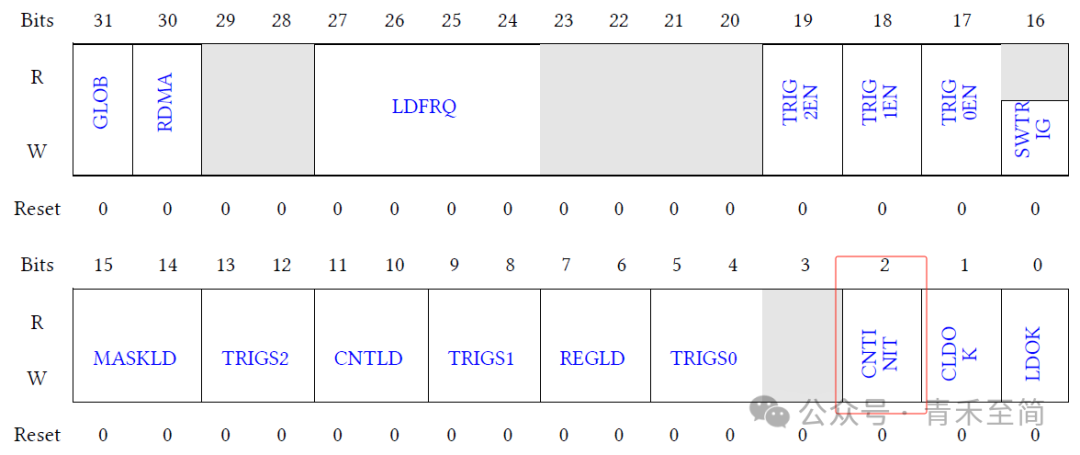
- SYNC[CNTINIT] is used to select the initial counting value of the counter:
- 0b – The initial counting value of the counter comes from the CNT register;
- 1b – The initial counting value of the counter comes from the INIT register;
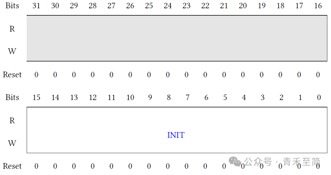
- INIT[INIT] is the initial counting value of the counter’s technical cycle. When SYNC[CNTINIT]=1, after enabling the counter (i.e., after CTRL[EN]=1), the starting value of the first counting cycle begins from INIT[INIT].
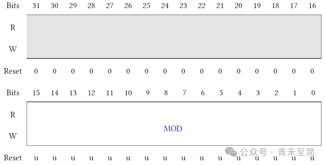
- MOD[MOD] is the counter’s modulus value, i.e., the maximum counting value.
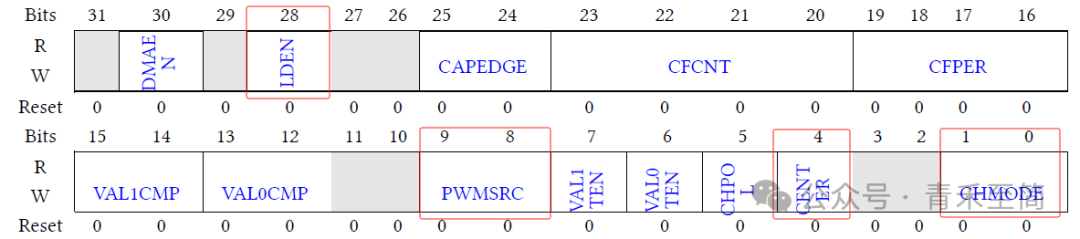
 (3) Channel Control Register Fields
- CH_CTRL[CHMODE] is the channel mode selection:
- 00b – General Timer mode
- 01b – PWM mode
- 10b – Comparison output mode
- 11b – Capture mode
- CH_CTRL[CENTER] is for center-aligned PWM type (the prerequisite is to configure the channel as PWM mode, i.e., CH_CTRL[CHMODE]=01b).
- CH_CTRL[PWMSRC] is the PWM driving source selection:
- 00b – Common mode, selecting the counter and CH_VAL0/CH_VAL1 match event as the PWM driving source.
- 01b – Inverted mode, using the inversion of the waveform in common mode as the PWM driving source.
- 10b – Software mode, configured through software as the PWM driving source (not commonly used, this article will not cover it).
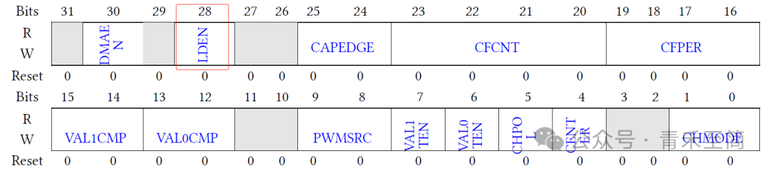
- CH_CTRL[LDEN] is the enable signal for the loading mechanism of CH_VAL0 and CH_VAL1 shadow registers, where CH_CTRL[LDEN=1 indicates whether the current channel’s related shadow registers participate in the loading mechanism.
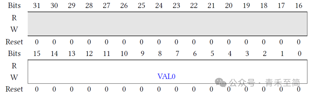
- CH_VAL0[VAL0] is the ‘0->1’ rising edge match point of the PWM, i.e., when the PWM driving source is configured to common mode, i.e., CH_CTRL[PWMSRC]=0, counter=CH_VAL0[VAL0] serves as the match event for the PWM’s ‘0->1’ rising edge.
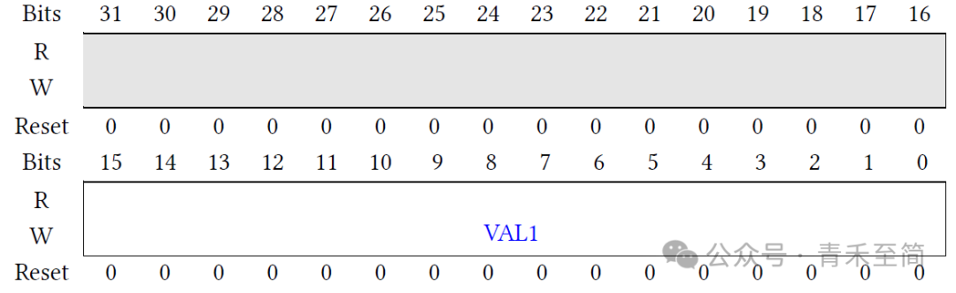
- CH_VAL1[VAL1] is the ‘1->0’ falling edge match point of the PWM, i.e., when the PWM driving source is configured to common mode, i.e., CH_CTRL[PWMSRC]=0, counter=CH_VAL1[VAL1] serves as the match event for the PWM’s ‘1->0’ falling edge.
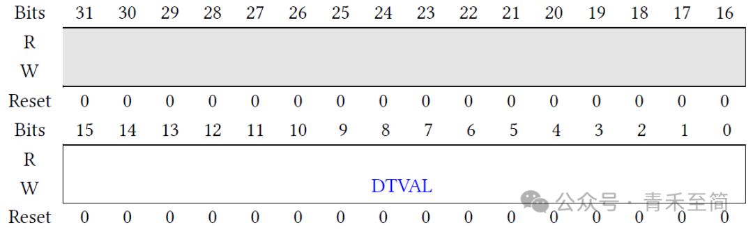
- CH_DT[DTVAL] is the dead time configuration in complementary mode. The PWM pairs generated in complementary mode, assuming the counter clock frequency is F_clock, have delays at the ‘0->1’ transition edge of: (CH_DT[DTVAL]+1)*CTRL[DTPRS]/F_clock, to avoid both PWMs being ‘1’ at the same time. Generally, motor applications require dead time configuration to be <5us, so CTRL[DTPRS]=0 is usually configured. The shorter the dead time, the higher the control accuracy. Sometimes, high-performance motor applications require an increase in dead time compensation algorithms. However, if the dead time is too short, it can cause heating, increased power consumption, and damage to power MOSFETs, so appropriate dead time should be configured.
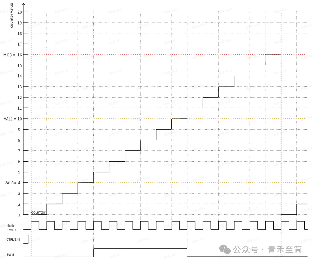
 2. Configuration and Types of PWM Generation(1) Asymmetric PWM, where the rising and falling edges are configured simultaneously, is configured as follows: MOD[MOD]=16; INIT[INIT]=0; CH_VAL0[VAL0]=4; CH_VAL1[VAL1]=10; CTRL[CLKPRS]=0; CTRL[EN]=1.In this case, the PWM transitions from ‘0->1’ at counter=VAL0 and from ‘1->0’ at counter=VAL1. VAL0 comes from the value of CH_VAL0[VAL0], and VAL1 comes from the value of CH_VAL1[VAL1]. The PWM generation process is shown in the figure below:
 (2) Edge-aligned PWM, which includes left-aligned PWM and right-aligned PWM.
- Left-aligned PWM requiresCH_VAL0[VAL0]= INIT[INIT], configured as follows:
MOD[MOD]=16; INIT[INIT]=0; CH_VAL0[VAL0]=0; CH_VAL1[VAL1]=10; CTRL[CLKPRS]=0; CTRL[EN]=1.In this case, the PWM is set to ‘1’ at the beginning of the cycle and transitions from ‘1->0’ at counter=VAL1. VAL1 comes from the value of CH_VAL1[VAL1]. The PWM generation process is shown in the figure below: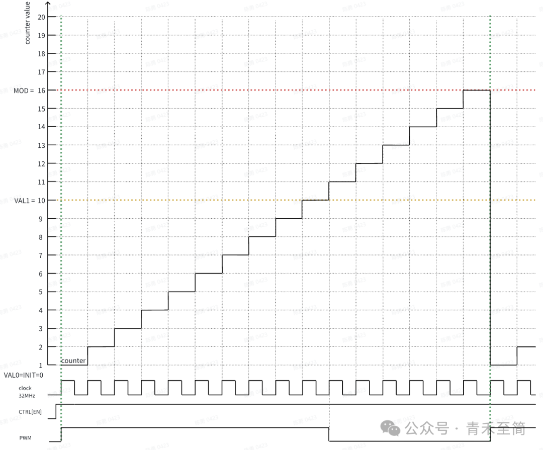
- Right-aligned PWM requiresCH_VAL1[VAL1]= MOD[MOD], configured as follows:
MOD[MOD]=16; INIT[INIT]=0; CH_VAL0[VAL0]=4; CH_VAL1[VAL1]=16; CTRL[CLKPRS]=0; CTRL[EN]=1.In this case, the PWM transitions from ‘0->1’ at counter=VAL0 and remains ‘1’ until the end of the cycle. VAL0 comes from the value of CH_VAL0[VAL0]. The PWM generation process is shown in the figure below: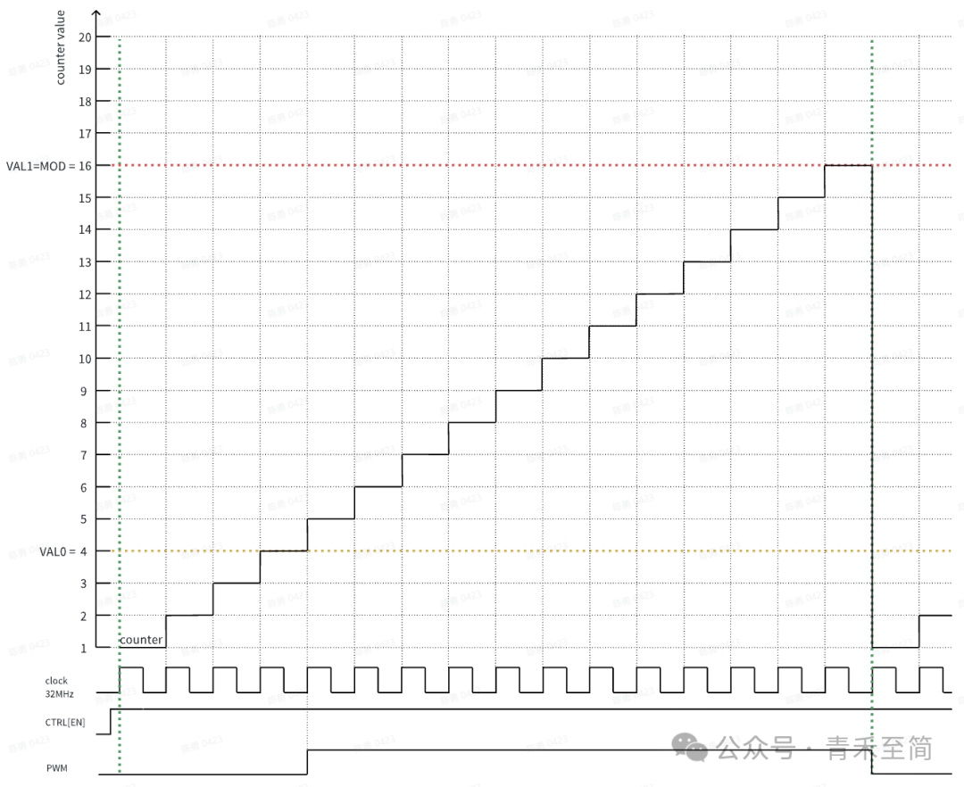 (3) Center-aligned PWM is commonly used in motor control FOC algorithms. eTMR can achieve center-aligned PWM through both software and hardware methods.
- When CH_CTRL[CENTER]=0, center-aligned PWM can be generated by calculating and configuring asymmetric PWM through software. The steps are as follows:
- The technical cycle is MOD[MOD]-INIT[INIT], and the duty cycle is duty.
- Calculate CH_VAL0[VAL0] and CH_VAL1[VAL1]:CH_VAL0[VAL0]=(1-duty)*(MOD[MOD]-INIT[INIT])/2CH_VAL1[VAL1]=(1+duty)*(MOD[MOD]-INIT[INIT])/2
- When CH_CTRL[CENTER]=1, center-aligned PWM is automatically generated through hardware. By writing a temporary value “VAL0_buf” to the register CH_VAL0[VAL0], where “VAL0_buf” represents the duration for which the center-aligned PWM remains ‘1’, the actual duty cycle is duty=VAL0_buf/(MOD[MOD]-INIT[INIT]). The digital circuit will automatically calculate CH_VAL0[VAL0] and CH_VAL1[VAL1] based on the temporary value VAL0_buf to generate center-aligned PWM.Configured as follows:MOD[MOD]=16;INIT[INIT]=0;Write the value VAL0_buf=8 to the CH_VAL0[VAL0] register;
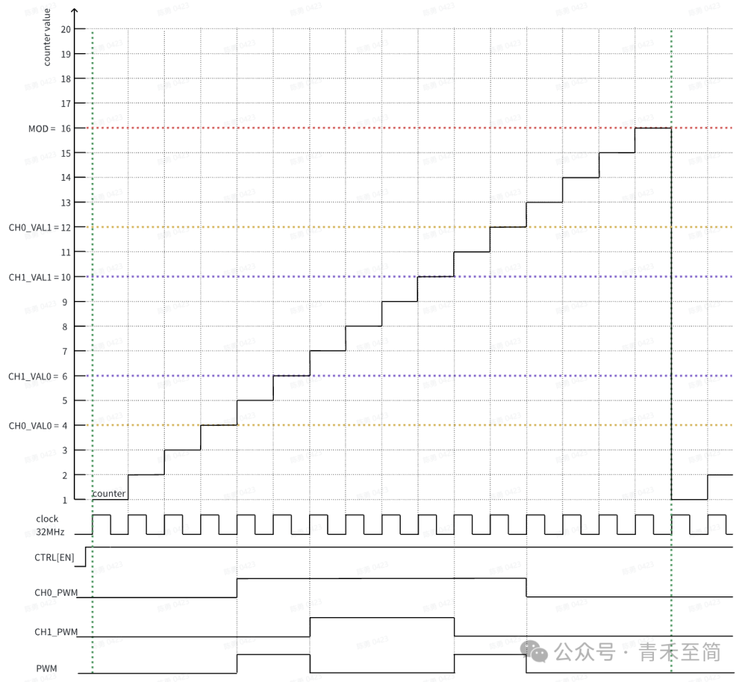
CTRL[CLKPRS]=0; CH_CTRL[CENTER]=1; CTRL[EN]=1.The hardware digital circuit calculates the values of CH_VAL0[VAL0] and CH_VAL1[VAL1]:CH_VAL0[VAL0]=[(MOD[MOD]+INIT[INIT])-VAL0_buf]/2=4;CH_VAL1[VAL1]=[(MOD[MOD]+INIT[INIT])+VAL0_buf]/2=12;In this case, the PWM transitions from ‘0->1’ at counter=VAL0 and from ‘1->0’ at counter=VAL1. VAL0 comes from the value of CH_VAL0[VAL0], and VAL1 comes from the value of CH_VAL1[VAL1]. The PWM generation process is shown in the figure below: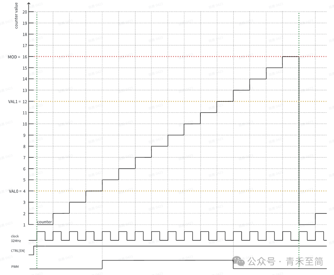 (4) Windowed PWM is generally used in complementary mode (which will be described in detail later), with windowed PWM serving as the source signal for complementary outputs.If configured in independent mode, ch0 and ch1 will output the same windowed PWM signal.The eTMR module’s channels can be configured as 8 independent channels ch0, ch1, ch2, …, ch7. They can also be configured as 4 paired channels, i.e., ch0/ch1, ch2/ch3, ch4/ch5, ch6/ch7. The windowed PWM is generated by the XOR ‘^’ logic of two paired channels, such as ch0/ch1, where the windowed PWM is “CH0_PWM ^ CH1_PWM”. This is used for windowing operations in motor applications.For example, for ch0/ch1, configured as follows: MOD[MOD]=16; INIT[INIT]=0; CH0_VAL0[VAL0]=4; CH0_VAL1[VAL1]=12; CH1_VAL0[VAL0]=6; CH1_VAL1[VAL1]=10; CTRL[DBSW01]=1; CTRL[CLKPRS]=0; CTRL[EN]=1.
 3. Loading Mechanism of Shadow Registers(1) Detailed Explanation of Related Register Configuration
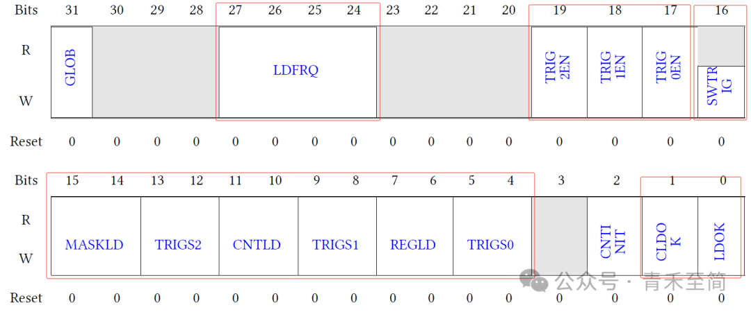
- SYNC[LDOK] and SYNC[CLDOK], writing ‘1’ to SYNC[LDOK] via APB can set SYNC[LDOK] to ‘1’, and writing ‘1’ to SYNC[CLDOK] via APB can clear SYNC[LDOK]. SYNC[CLDOK] automatically clears after SYNC[LDOK] is cleared. When SYNC[LDOK]=0, shadow registers can be written to; when SYNC[LDOK]=1, write operations will be invalid, serving as a protection mechanism. If you wish to perform write operations again, you need to write ‘1’ to SYNC[CLDOK] to clear SYNC[LDOK], and then perform write operations again.
- SYNC[REGLD] and SYNC[TRIGS0] are used to configure the loading events for INIT, MID, MOD, CHxVAL0, and CHxVAL1 shadow registers. The configuration of SYNC[REGLD] is as follows:
- 00b – Disable loading event
- 01b – MOD match event, i.e., at the moment counter=MOD[MOD]
- 10b – MID match event, i.e., at the moment counter=MID[MID]
- 11b – Trigger event, selected via SYNC[TRIGS0]
SYNC[TRIGS0] configuration is as follows:
- 00b – Disable trigger event
- 01b – Select SW trigger event
- 10b – Select HW trigger event, any HW trigger0/1/2 event
- 11b – Select any SW/HW trigger event
- SYNC[CNTLD] and SYNC[TRIGS1] are used to configure the counter loading events. SYNC[CNTLD] configuration is as follows:
- 00b – Maintain consistency with the loading events of INIT, MID, MOD, CHxVAL0, and CHxVAL1 shadow registers.
- 01b – MID match event, i.e., at the moment counter=MID[MID]
- 10b – Trigger event, selected via SYNC[TRIGS1]
SYNC[TRIGS1] configuration is as follows:
- 00b – Disable trigger event
- 01b – Select SW trigger event
- 10b – Select HW trigger event, any HW trigger0/1/2 event
- 11b – Select any SW/HW trigger event
- SYNC[MASKLD] and SYNC[TRIGS2] are used to configure the CHMASK shadow register loading events. SYNC[MASKLD] configuration is as follows:
- 00b – Maintain consistency with the loading events of INIT, MID, MOD, CHxVAL0, and CHxVAL1 shadow registers.
- 01b – MOD match event, i.e., at the moment counter=MOD[MOD]
- 10b – MID match event, i.e., at the moment counter=MID[MID]
- 11b – Trigger event, selected via SYNC[TRIGS2]
SYNC[TRIGS2] configuration is as follows:
- 00b – Disable trigger event
- 01b – Select SW trigger event
- 10b – Select HW trigger event, any HW trigger0/1/2 event
- 11b – Select any SW/HW trigger event
- SYNC[SWTRIG] is for SW trigger events. Writing ‘1’ to SYNC[SWTRIG] via APB will generate a SW trigger event. After the hardware generates a valid trigger, it will automatically clear it, and reading SYNC[SWTRIG] will return a value of 0.
- SYNC[TRIG0EN]/SYNC[TRIG1EN]/SYNC[TRIG2EN] are the enable bits for HW triggers. After enabling, any trigger arrival will generate a HW trigger event, with triggers coming from the TMU.
- SYNC[LDFRQ] is the loading frequency, i.e., after SYNC[LDFRQ] loading events occur, the shadow register loading is completed. This is usually configured when the MCU performance for motor control is poor, and the calculation time is long, ensuring that the loading occurs after a delay to guarantee calculation time, or when the motor control precision is not high, it can also be configured to complete loading after several cycles.
- CHx_CTRL[LDEN] is used to enable channel CHx loading, allowing CHxVAL0/CHxVAL1 to participate in loading.
 (2) The fundamental principle of shadow registers is to use dual-buffer registers buffer 1 and buffer 2, where the access addresses of dual-buffer registers buffer 1 and buffer 2 are the same. The core writes to the addr address via the APB bus to configure the value of buffer 1; at a specific controllable loading point (or loading event), the value in the buffer 1 register is loaded into the buffer 2 register. The core reads the addr address via the APB bus, and the returned value is from the buffer 2 register. For a specific shadow register, the value of buffer 1 is usually configured through the APB bus as a preparatory value, which is immediately assigned to buffer 2 at the loading event, and the value of buffer 2 is used in the working area. The benefit of this is that it allows for pre-configured values to take effect at a specific time. For several shadow registers, all buffer 1 values are configured sequentially through the APB bus, and when the loading event occurs, all preparatory values are loaded into buffer 2 simultaneously, taking effect at the same time. This avoids the delay caused by switching configurations through the APB bus, which is very necessary in applications. For example, motor control expects PWM to switch duty cycles simultaneously over a full cycle or to switch states at the same time.eTMR includes shadow registers such as INIT, MOD, MID, CHxVAL0, CHxVAL1, CHMASK, where MID is mainly used to generate trigger events, which can be used for real-time triggering of ADC conversions, etc. This will not be described further here. CHMASK is used to mask the output PWM signals in real-time, which can be seen as a safety mechanism. For example, if a fault is detected, the motor can be temporarily placed in a safe state, or it can be used as a PWM control method. Detailed descriptions will be provided in subsequent chapters.The configuration process is as follows:
- Write ‘1’ to SYNC[CLDOK] via APB to clear SYNC[LDOK]. When the condition SYNC[LDOK]=0 is met, shadow registers can be written to via APB. Otherwise, write operations will be invalid.
- When SYNC[LDOK]=0, configure all shadow registers’ buffer 1 via APB.
- After the write operation is completed, write ‘1’ to SYNC[LDOK] via APB to set SYNC[LDOK]. At this point, no further write operations can be performed via APB, and write operations will be considered invalid, serving as a write protection mechanism.
- Wait for the arrival of the loading event, which includes:
- MOD match, i.e., when counter=MOD[MOD].
- MID match, i.e., when counter=MID[MID].
- HW trigger, hardware trigger events, HW triggers come from the TMU module.
- SW trigger, software trigger events, generated by writing ‘1’ to SYNC[SWTRIG] via APB.
- HW/SW trigger, hardware or software trigger events, any event occurrence triggers the loading event.
- When the loading event arrives and SYNC[LDOK]=1, the hardware automatically loads the values from all shadow registers’ buffer 1 into buffer 2. After loading is complete, the hardware automatically clears SYNC[LDOK].
The schematic diagram is as follows: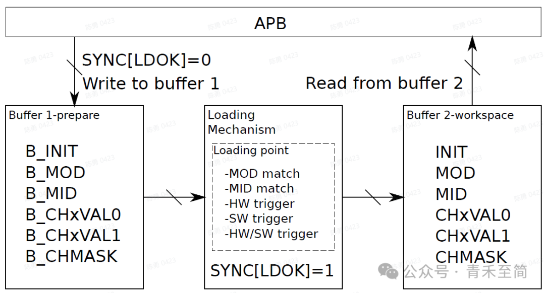 (3) Loading of INIT, MOD, MID, CH_VAL0, and CH_VAL1 registers for a full cycle, configured as follows:SYNC[REGLD]=01b
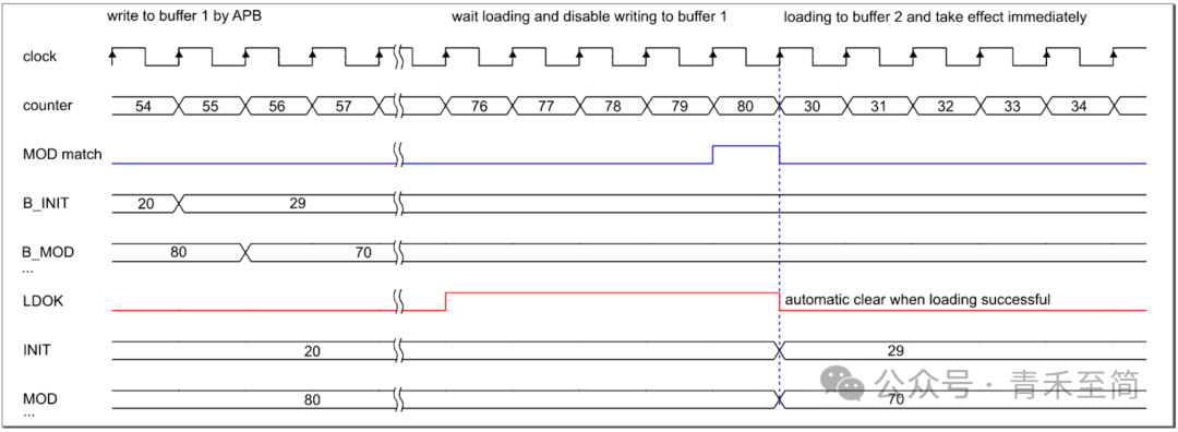
- In the previous cycle, INIT=20, MOD=80
- When SYNC[LDOK]=0, update INIT=29, MOD=70 corresponding to buffer 1.
- SYNC[LDOK]=1
- Wait for the loading event to occur when counter=MOD, the next cycle will beINIT=29, MOD=70, SYNC[LDOK] automatically cleared,as shown in the figure below:
 (4) Loading of INIT, MOD, MID, CH_VAL0, and CH_VAL1 registers via HW trigger events, configured as follows:SYNC[REGLD]=11bSYNC[TRIGS0]=10b
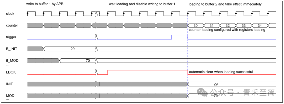
- In the previous cycle, INIT=xx, MOD=xx
- When SYNC[LDOK]=0, update INIT=29, MOD=70 corresponding to buffer 1.
- SYNC[LDOK]=1
- Wait for the HW trigger loading event to occur, the next cycle will change toINIT=29, MOD=70, SYNC[LDOK] automatically cleared,as shown in the figure below:
 (5) Loading of the CHMASK register is similar to the loading of INIT, MOD, MID, CH_VAL0, and CH_VAL1 registers, and will not be elaborated further here.(6) Loading of the counter is similar to the loading of INIT, MOD, MID, CH_VAL0, and CH_VAL1 registers, with the loading value coming from the INIT register value. When counter=MOD, the loading of the INIT value will always be completed.4. ConclusionThis article provides a detailed explanation of the principles of PWM generation, including the types of PWM generated: edge-aligned PWM, center-aligned PWM, asymmetric PWM, and windowed PWM types; the loading mechanism of shadow registers, etc. The next part will describe independent mode and complementary mode; the dead time of complementary mode; and designs related to motor safety, etc.If you have any questions, please feel free to criticize and provide feedback, let’s communicate and improve together~