In recent years, with the continuous promotion of China’s new infrastructure and “Made in China 2025”, it has become increasingly difficult for single ARM processors to meet the functional requirements of industrial sites. Particularly in industries such as energy, industrial control, and smart medical care, a processor platform based on ARM+FPGA architecture is often needed to achieve specific functions, such as multi-channel/high-speed AD acquisition, multiple network ports, multiple serial ports, multi-channel/high-speed parallel DI/DO, and high-speed data parallel processing.
What advantages does the ARM+FPGA architecture have?
ARM: Rich in interface resources, low power consumption, and excels in multimedia display and logic control.
FPGA: Excels in multi-channel or high-speed AD acquisition, interface expansion, high-speed signal transmission, and high-speed data parallel processing.
Therefore, the ARM+FPGA architecture can provide comprehensive advantages in performance, cost, and power consumption. ARM and FPGA can not only perform their respective roles, leveraging their unique advantages, but also collaborate to address more complex issues.
For cost-insensitive and high-speed communication applications, a PCIe communication interface is generally used. However, for cost-sensitive ARM+FPGA applications, the PCIe communication interface can keep the cost of FPGA chips high.
In many industrial fields such as energy and industrial control, what is truly needed is a solution that is competitive in both performance and cost, capable of achieving high-speed communication between ARM and FPGA while also being cost-optimal, preferably based on domestic solutions.
In this context of demand, Tronlong Technology provides three solutions for high-speed communication based on domestic ARM and low-cost FPGA.
This article mainly introduces three high-speed communication solutions based on SPI, SDIO, and CSI between Allwinner Technology T3/A40i and Unisoc PGL25G/Xilinx Spartan-6, with a maximum communication speed of up to 55.1MB/s.
To simplify the description, this article only extracts the functional descriptions and test results of the solutions. For detailed development documentation (case source code), please long press the QR code below to download the materials.

* Hardware Platform Introduction (Allwinner Technology T3/A40i)
Tronlong Technology TLT3-EVM/TLA40i-EVM is a 4-core ARM Cortex-A7 domestic industrial evaluation board designed based on the Allwinner Technology T3/A40i processor, with a maximum frequency of 1.2GHz per core, consisting of a core board and an evaluation baseboard. T3 and A40i are pin-to-pin compatible.
The evaluation board has rich interface resources, providing dual network ports, dual CAN, dual USB, dual RS485 communication interfaces, and onboard Bluetooth, WIFI, and 4G (optional) modules. It also provides multimedia interfaces such as MIPI LCD, LVDS LCD, TFT LCD, HDMI OUT, CVBS OUT, CAMERA, LINE IN, H/P OUT, supports dual-screen display, Mali400 MP2 GPU, 1080P@45fps H.264 hardware encoding, 1080P@60fps H.264 hardware decoding, and supports SATA large-capacity storage interfaces.
The core board uses a 100% domestic component solution and has undergone professional PCB layout and high/low temperature testing verification, ensuring stability and reliability to meet various industrial application environments. Most components on the evaluation baseboard use domestic solutions, facilitating rapid product solution evaluation and technical research for users.
1 spi_rw Case
1.1 Case Description
Case Function: Mainly demonstrates SPI communication between T3/A40i (ARM Cortex-A7) and PGL25G/Spartan-6 (FPGA) processors.
ARM Side Implements SPI Master Function
a. Open the SPI device node, e.g., /dev/spidev0.0.
b. Use ioctl to configure the SPI bus, such as SPI bus polarity and phase, communication rate, data word length, etc.
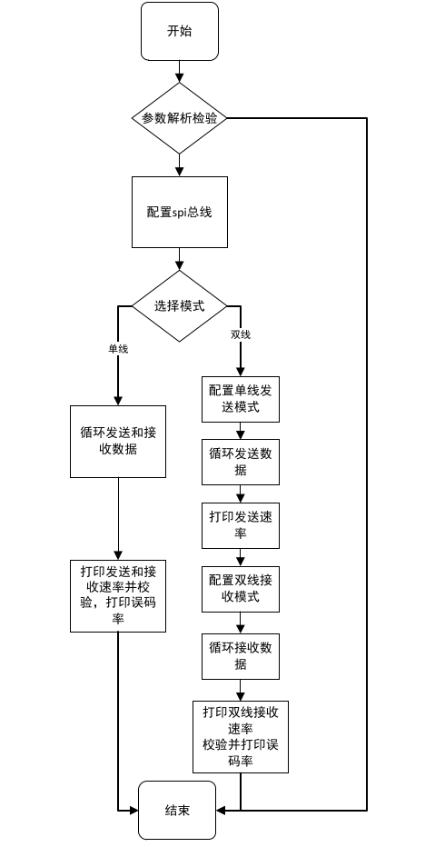
c. Choose mode as single-line mode or dual-line mode. When the SPI bus is in dual-line mode, sending data is in single-line mode, and receiving data is in dual-line mode.
d. Send data to the SPI bus and read data from the SPI bus. (Note: If the data for a single transfer exceeds 64Byte, the driver will automatically enable DMA transfer functionality.)
e. Print sending and receiving rates.
f. Verify read and write data, then print the error rate.
FPGA Side Implements SPI Slave Function
a. FPGA saves the 2KByte data sent by the SPI Master to BRAM.
b. When the SPI Master initiates a read, the FPGA reads 2KByte from BRAM and transmits it to the SPI Master via the SPI bus.
c. When the SPI bus is in dual-line mode, receiving data supports dual-line mode, while sending data does not support dual-line mode.
Figure 1 ARM Side Program Flowchart
According to the official data manual, the theoretical maximum clock frequency for SPI bus communication is 100MHz. This test specifies the SPI bus communication clock frequency at the maximum of 100MHz, thus the theoretical rate for SPI single-line mode is: (100000000/1024/1024/8)MB/s ≈ 11.92MB/s. The measured SPI single-line mode write rate is: 10.924MB/s, and the SPI single-line mode read rate is: 10.924MB/s.
According to the official data manual, the theoretical maximum clock frequency for SPI bus communication is 100MHz. This test specifies the SPI bus communication clock frequency at the maximum of 100MHz, thus the theoretical rate for SPI single-line mode is: (100000000/1024/1024/8)MB/s ≈ 11.92MB/s; the theoretical rate for SPI dual-line mode is: (100000000/1024/1024/4)MB/s ≈ 23.84MB/s. The measured SPI single-line mode write rate is 11.631MB/s, and the SPI dual-line mode read rate is 17.807MB/s.
2 rt_spi_rw Case
Case Function: Based on the Linux-RT system, demonstrates SPI communication between T3/A40i (ARM Cortex-A7) and PGL25G/Spartan-6 (FPGA) processors (single-line mode).
ARM Side Implements SPI Master Function
a. Open the SPI device node, e.g., /dev/spidev0.0.
b. Use ioctl to configure the SPI bus, such as SPI bus polarity and phase, communication rate, data word length, etc.
c. Create a real-time thread.
d. Send data to the SPI bus and read data from the SPI bus.
e. Print sending, receiving rates, and transmission time.
f. Verify read and write data, then print the error rate.
FPGA Side Implements SPI Slave Function
a. FPGA saves the 2KByte data sent by the SPI Master to BRAM.
b. When the SPI Master initiates a read, the FPGA reads 2KByte from BRAM and transmits it to the SPI Master via the SPI bus.

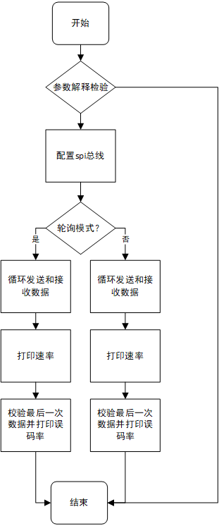
Figure 2 ARM Side Program Flowchart
According to the official data manual, the theoretical maximum clock frequency for SPI bus communication is 100MHz. This test specifies the SPI bus communication clock frequency at the maximum of 100MHz, thus the theoretical rate is: (100000000/1024/1024/8)MB/s ≈ 11.92MB/s. The minimum time for transmitting 4Byte data is 49us, the maximum time is 662us, and the average time is 227us; the write rate is 0.017MB/s, and the read rate is 0.017MB/s.
According to the official data manual, the theoretical maximum clock frequency for SPI bus communication is 100MHz. This test specifies the SPI bus communication clock frequency at the maximum of 100MHz, thus the theoretical rate is: (100000000/1024/1024/8)MB/s ≈ 11.92MB/s. The minimum time for transmitting 4Byte data is 14us, the maximum time is 59us, and the average time is 14us; the write rate is 0.239MB/s, and the read rate is 0.239MB/s.
3 sdio_test Case
Case Function: Demonstrates SDIO communication between T3/A40i (ARM Cortex-A7) and PGL25G/Spartan-6 (FPGA) processors.
ARM Side Implements SDIO Master Function
a. Open the SDIO device node, e.g., /dev/generic_sdio0.
b. Send data to the SDIO bus and read data from the SDIO bus.
c. Print sending and receiving rates.
d. Verify read and write data, then print the error rate.
FPGA Side Implements SDIO Slave Function
a. FPGA saves the 2KByte data sent by the SDIO Master to BRAM.
b. When the SDIO Master initiates a read, the FPGA reads 2KByte from BRAM and transmits it to the SDIO Master via the SDIO bus.

Figure 3 ARM Side Program Flowchart
This test specifies the SDIO bus communication clock frequency at 25MHz (maximum 50MHz), thus the theoretical communication rate is: (25 x 4 / 8)MB/s = 12.5MB/s. The measured write rate is 5.113MB/s, the read rate is 5.440MB/s, with an error rate of 0.0%.
4 csi_test Case
Case Function: Demonstrates CSI communication between T3/A40i (ARM Cortex-A7) and PGL25G/Spartan-6 (FPGA) processors.
a) Based on Linux subsystem V4L2.
b) Collect specified frame data through the CSI bus.
d) Print average collection rate and verify the data of the last frame image.
a) Write test data (0x00 ~ 0xFF) into FIFO.
b) Read data from FIFO, sending it to the ARM side via the CSI bus in a line and frame manner, at a resolution of 1024 x 512.
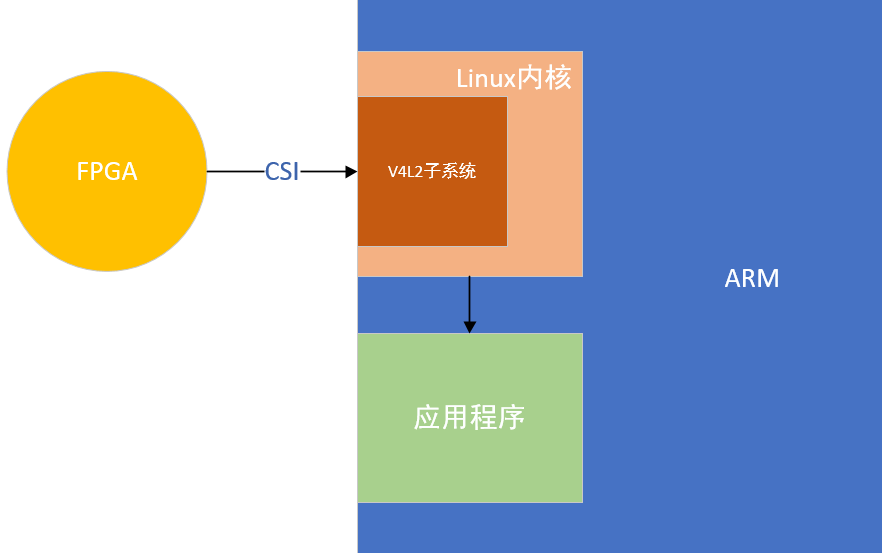
The CSI bus used is CSI0, supporting a maximum resolution of 1080P30, with a data width of 8bit. The functional block diagram and program flowchart are shown below.

Figure 4 Functional Block Diagram

Figure 5 ARM Side Program Flowchart
FPGA side sets CSI_PCLK to 65MHz, and the clock FIFO_WR_CLK for writing test data to FIFO is set to 59MHz. Since the FPGA side must write data to FIFO and then read it out to send, the interval time between each line and each frame will be affected by the FIFO writing rate, so the actual theoretical transmission bandwidth for CSI communication should be: (59MHz x 8bit / 8)MB/s = 59MB/s. The measured transmission rate is 55.1MB/s, with an error rate of 0.0%.
For more details, please see detailed case descriptions/ test methods, case source code,
please long press or scan the QR code to download

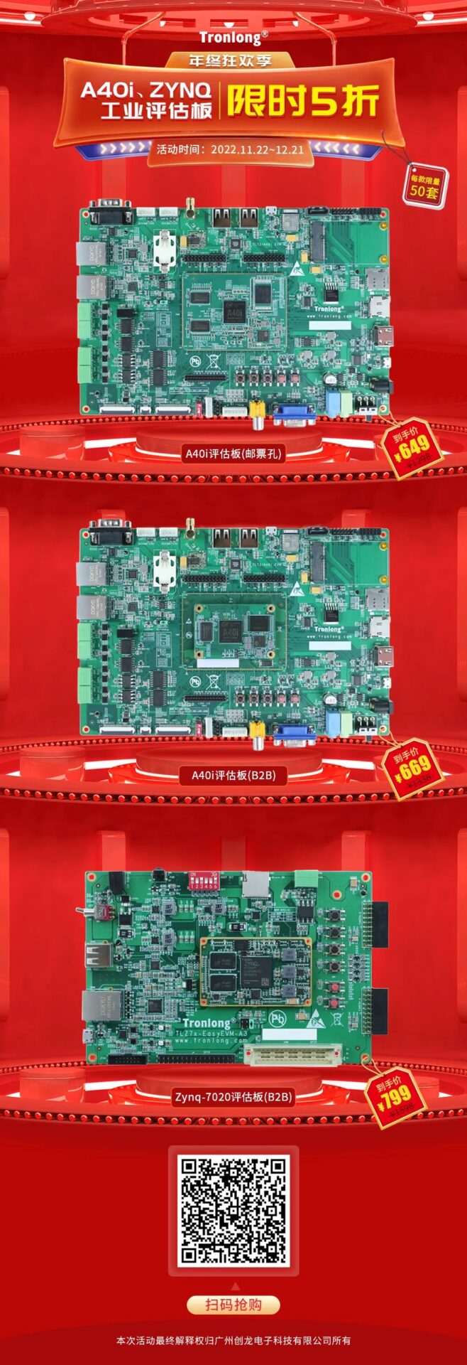
Recently, Tronlong Technology has launched a year-end “50% Off Promotional Board” activity, all domestic ARM and ZYNQ series development boards are available! Limited to 50 sets, first come, first served, interested friends can take a look.
Click the Tmall link: https://tronlong.tmall.com
or search on Taobao: tronlong flagship store
Quickly refresh your equipment library!
November 22, 2022 – December 21, 2022
a) Each Taobao ID and each item is limited to one set;
b) This 50% off activity is only available in Tmall Mall, and offline purchases do not enjoy this activity discount.
Note: Currently, Tronlong Technology has launched the T3/A40i+PGL25G fully domestic integrated industrial core board solution, with a domestic rate of 100% (connectors are also domestic). If needed, please consult Tronlong Technology.
Figure 6 T3/A40i+PGL25G Fully Domestic Industrial Core Board


Contact Tronlong Technology:
Tronlong Switchboard: 020-8998-6280
Technical Hotline: 020-3893-9734
Tronlong Official Website: www.tronlong.com
Technical Forum: www.51ele.net
Official Mall: https://tronlong.tmall.com


