1. What is UART?
UART, as one of the three commonly used low-speed buses (UART, SPI, IIC), plays an important role in designing various communication interfaces and debugging.
UART stands for Universal Asynchronous Receiver/Transmitter, which is mainly used for serial data transmission between devices and operates in a full-duplex mode.
When sending data, it converts parallel data into serial data for transmission, and when receiving data, it converts the received serial data back into parallel data.
The term “asynchronous” means that a synchronous clock is not used between the two modules involved in data transmission.
In fact, asynchronous serial transmission does not require a clock; instead, it uses specific timing to indicate the start (start bit – from high to low) and end (stop bit, pulled high) of transmission.
2. Components of UART
2.1 Physical Layer of UART
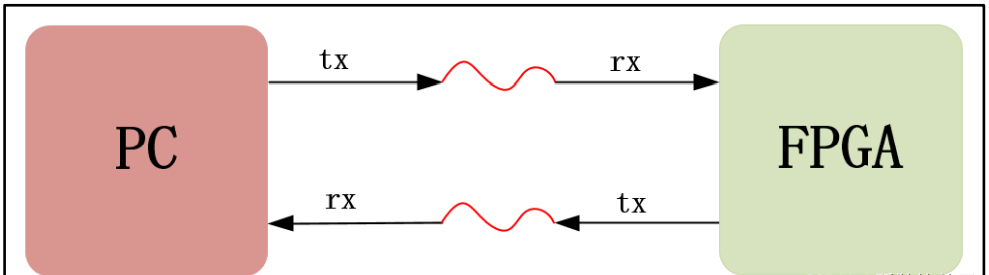
UART communication consists of only two signal lines: one for transmitting data called tx (Transmitter) and one for receiving data called rx (Receiver).
As shown in the figure, for a PC, its tx must connect to the rx of the FPGA, and similarly, the rx of the PC must connect to the tx of the FPGA. If two tx or two rx are connected, data cannot be sent or received properly.
The transmission of signals is implemented by external driver circuits. The transmission process of electrical signals has different level standards and interface specifications. The interface standards for asynchronous serial communication include RS232, RS422, RS485, etc.
These standards define different electrical characteristics of the interfaces, such as RS-232 being single-ended input/output, while RS-422/485 are differential input/output.
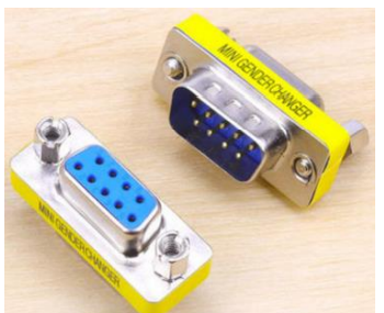
For short transmission distances (not exceeding 15m), RS232 is the most commonly used interface standard for serial communication. The most common interface type for RS-232 is DB9, as shown in the figure. Industrial control computers generally come equipped with multiple serial ports, and many older desktop computers also have serial ports.
However, laptops and newer desktop computers typically do not have serial ports; they usually achieve serial communication with external devices through USB-to-serial cables.
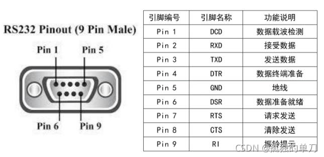
The DB9 interface definition and the function description of each pin are shown in the figure. We generally only use pins 2 (RXD), 3 (TXD), and 5 (GND); other pins are usually not used in standard serial mode:
2.2 UART Protocol
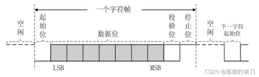
A frame of data in UART during the sending or receiving process consists of four parts: start bit, data bits, parity bit, and stop bit, as shown in the figure.
The start bit indicates the beginning of a frame of data, while the stop bit indicates the end of a frame of data, and the data bits contain the valid data.
The parity bit can be either odd or even, used to check for errors in data transmission.
In odd parity, the sender ensures that the total number of 1s in the data bits plus the parity bit is odd; the receiver checks the number of 1s upon receiving the data.
If it is not odd, it indicates that an error occurred during transmission. Similarly, even parity checks whether the number of 1s is even. For more information on odd and even parity, refer to: FPGA Odd/Even Parity Implementation in Verilog.
The data format and transmission rate in UART communication are configurable. For correct communication, both the sender and receiver must agree on and adhere to the same settings.
Data bits can be selected as 5, 6, 7, or 8 bits, with 8 bits being the most commonly used in practical applications; parity bits can be odd, even, or none; and stop bits can be 1 (default), 1.5, or 2 bits.
The baud rate represents the speed of serial communication, indicating the number of bits transmitted per second, measured in bps (bits per second). Common baud rates include 9600, 19200, 38400, 57600, and 115200.
For example, a baud rate of 9600 means that 9600 bits of data are transmitted per second. Considering that sending one byte takes 10 bits (1 start bit + 8 data bits + 1 stop bit + no parity bit), the time required to transmit one byte is 1*10/9600 seconds.
3. UART Transmission Module
3.1 Interface Definition and Overall Design
The overall block diagram of the transmission module, along with input and output signals, is shown below:
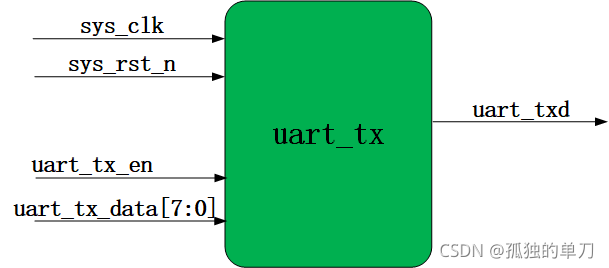
The signal ports are as follows:
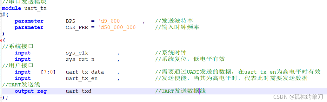
It should be noted that uart_tx_data is the byte of data to be sent, and uart_tx_en is the transmission enable signal. When it is pulled high, it indicates that data uart_tx_data is being sent through the serial transmission line.
3.2 Design Concept
This module supports the transmission of any baud rate (theoretically), but it needs to be instantiated with parameters when using this module, with 8 data bits, 1 start bit, and 1 stop bit, with no parity.
When the enable signal is valid, the transmission flag signal is pulled high, indicating that the module has entered the transmission process; after sending 10 bits, the transmission flag signal is pulled low, indicating the end of the transmission process. The data to be sent is stored when the enable signal is valid.
Assuming a baud rate of 9600, the time to send one bit is 1s/9600, and a data transmission consists of 10 bits (8 data bits, 1 start bit, and 1 stop bit), thus requiring 1s/9600 seconds in total.
Assuming the system clock is 50MHz (parameterized to adapt to different system frequencies), its period is 20ns, so the number of system cycles required to send one bit is (1s/9600)/20ns ≈ 5208 cycles.
A counter is used during the transmission process to count, with a range of (0~5208-1), which corresponds to 10 intervals (one byte requires sending 10 bits);
Additionally, another counter is needed to count the number of bits sent (each time the previous counter reaches 5207, it indicates that one bit has been sent), with a range of (0~9).
During the transmission process, based on the value of the counter (bit count), the transmission data line is operated.
If the bit count = 0, it indicates that the start bit needs to be sent;
If the bit count = 1, it indicates that the least significant bit (LSB) of the data needs to be sent (data is always sent with the low bit first, followed by the high bit);
······
If the bit count = 8, it indicates that the most significant bit (MSB) of the data needs to be sent;
If the bit count = 9, it indicates that the stop bit needs to be sent;
The transmission data line must be pulled high when not in transmission state to meet the idle state of UART timing.
3.3 Verilog Code
Based on the above design concept, part of the transmission module code is as follows:
// *******************************************************************************************************// ** Author : Lonely Sword // ** Email : [email protected]// ** Blog : https://blog.csdn.net/wuzhikaidetb // ** Date : 2022/07/31 // ** Function : 1. UART transmission driver module based on FPGA; // 2. Configurable baud rate BPS, main clock CLK_FRE; // 3. 1 start bit, 8 data bits, 1 stop bit, no parity; // 4. After sending 1 byte, pull uart_tx_done high for one cycle, can be used for subsequent multi-byte transmission modules. // ******************************************************************************************************* module uart_tx#( parameter integer BPS = 9_600 , // Baud rate parameter integer CLK_FRE = 50_000_000 // Main clock frequency)(// System interface input sys_clk , // System clock input sys_rst_n , // System reset, active low // User interface input [7:0] uart_tx_data , // Data to be sent via UART, valid when uart_tx_en is high input uart_tx_en , // Transmission valid, when high, indicates that the data to be sent is valid // UART transmission output reg uart_tx_done , // Pull high for one cycle after successfully sending 1 BYTE output reg uart_txd // UART transmission data line tx); // When the transmission enable signal arrives, store the data to be sent to avoid subsequent changes or loss always @(posedge sys_clk or negedge sys_rst_n)begin if(!sys_rst_n) uart_tx_data_reg <=8'd0; else if(uart_tx_en) // Valid data to be sent uart_tx_data_reg <= uart_tx_data; // Store the data to be sent else uart_tx_data_reg <= uart_tx_data_reg;end // When the transmission enable signal arrives, enter the transmission process always @(posedge sys_clk or negedge sys_rst_n)begin if(!sys_rst_n) tx_state <=1'b0; else if(uart_tx_en) tx_state <= 1'b1; // Enter transmission process when transmission signal is valid // Exit transmission process after the last data is sent else if((bit_cnt == BITS_NUM - 1'b1) && (clk_cnt == BPS_CNT - 1'b1)) tx_state <= 1'b0; else tx_state <= tx_state; end // After the transmission is complete, pull the transmission complete signal high for one cycle, indicating that one byte has been sent always @(posedge sys_clk or negedge sys_rst_n)begin if(!sys_rst_n) uart_tx_done <=1'b0; // Pull high for one cycle after transmission is complete else if((bit_cnt == BITS_NUM - 1'b1) && (clk_cnt == BPS_CNT - 1'b1)) uart_tx_done <=1'b1; else uart_tx_done <= 1'b0;end// After entering the transmission process, start the clock counter and bit count counter always @(posedge sys_clk or negedge sys_rst_n)begin if(!sys_rst_n)begin clk_cnt <= 32'd0; bit_cnt <= 4'd0; end else if(tx_state) begin // In transmission state if(clk_cnt < BPS_CNT - 1'd1)begin // A bit of data has not been sent yet clk_cnt <= clk_cnt + 1'b1; // Clock counter +1 bit_cnt <= bit_cnt; // Bit counter remains unchanged end else begin // A bit of data has been sent clk_cnt <= 32'd0; // Clear the clock counter, restart timing bit_cnt <= bit_cnt+1'b1; // Bit counter +1, indicating that one bit of data has been sent end end else begin // Not in transmission state clk_cnt <= 32'd0; // Clear bit_cnt <= 4'd0; // Clear endendendmodule3.4 Testbench
The design of the Testbench is as follows:
Set the baud rate to 230400 (this is to facilitate observing the transmission enable signal uart_tx_en and save time).
After 3000ns, pull the transmission enable signal uart_tx_en high for one cycle, while generating 1 random 8-bit data for uart_tx_data as the data to be sent.
Observe whether the timing on the TX line of UART meets the requirements.
// *******************************************************************************************************// ** Author : Lonely Sword // ** Email : [email protected]// ** Blog : https://blog.csdn.net/wuzhikaidetb // ** Date : 2022/07/29 // ** Function : 1. Testbench for the UART transmission driver module based on FPGA // 2. Send one 8-bit random data, observe whether its waveform meets UART timing requirements // ******************************************************************************************************* `timescale 1ns/1ns // Define time scale module tb_uart_tx(); reg sys_clk ; reg sys_rst_n ; reg [7:0] uart_tx_data ;reg uart_tx_en ; wire uart_txd ; parameter integer BPS = 'd230400 ; // Baud rate parameter integer CLK_FRE = 'd50_000_000 ; // System frequency 50M localparam integer BIT_TIME = 'd1000_000_000 / BPS ; // Calculate the time required to transmit each bit initial begin sys_clk <=1'b0; sys_rst_n <=1'b0; uart_tx_en <=1'b0; uart_tx_data <=8'd0; #80 // System starts working sys_rst_n <=1'b1; #200 @(posedge sys_clk); uart_tx_en <=1'b1; uart_tx_data <= ({$random} % 256); // Send 8-bit random data #20 uart_tx_en <=1'b0; #(BIT_TIME * 10) // Sending 1 BYTE requires 10 bits #200 $finish; // End simulation end always #10 sys_clk=~sys_clk; // Define main clock, period 20ns, frequency 50M // Instantiate the transmission driver module uart_tx #( .BPS (BPS ), .CLK_FRE (CLK_FRE ) ) uart_tx_inst( .sys_clk (sys_clk ), .sys_rst_n (sys_rst_n ), .uart_tx_data (uart_tx_data ), .uart_tx_en (uart_tx_en ), .uart_tx_done (uart_tx_done ), .uart_txd (uart_txd ) ); endmodule3.5 Simulation Result Analysis
The simulation results are shown in the figure below (with detailed comments):
In the figure below, it can be seen that the transmission module sent 1 data 8’h24, and after a period of time, the transmission ended, and the timing on the TX line could not be directly observed.
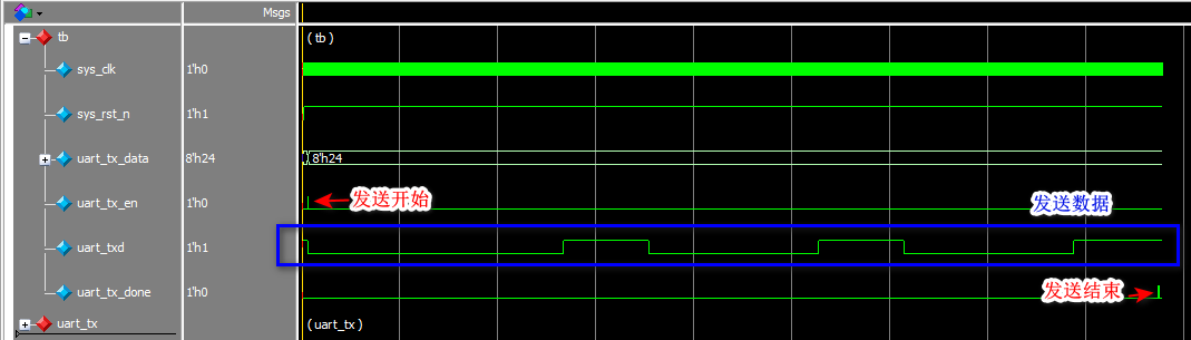
Overall simulation timing
In the figure below, it can be seen that the transmission module sent 1 data 8’h24, and after a period of time, the transmission ended, and the TX line sent data 00100100 (low bit first, high bit last) in accordance with UART timing, which is 8’h24.
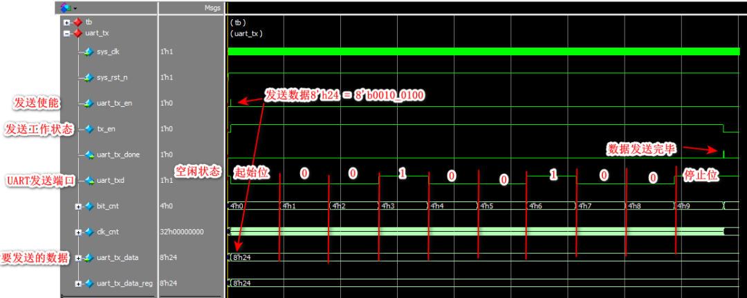
Single transmission timing
It can be seen that the simulation result meets the expected design requirements.
3.6 On-Board Testing
Having successfully completed the simulation verification of the transmission module, the next step is to conduct on-board testing using an Altera Cyclone IV E development board.
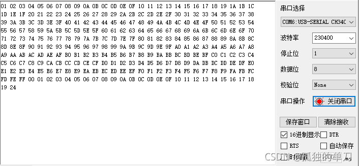
A test module for the transmission module is written, which calls the serial transmission module and pulls the transmission enable signal high at regular intervals (default 1s) while generating transmission data, starting from 0x01 and incrementing by 1 until 0xFF (overflowing to 0x00).
At the same time, a serial debugging software on the computer is used to receive the transmitted data. The success of the serial transmission module is determined based on the data received by the serial debugging software.
The verification module code for the transmission module is as follows:
// *******************************************************************************************************// ** Author : Lonely Sword // ** Email : [email protected]// ** Blog : https://blog.csdn.net/wuzhikaidetb // ** Date : 2022/07/29 // ** Function : 1. Test module for the UART transmission driver module based on FPGA; // 2. Send 1 incrementing data to the host every 1s. // ******************************************************************************************************* module uart_tx_test(// System interface input sys_clk , input sys_rst_n , // UART transmission line output uart_txd // UART transmission line); parameter integer BPS = 'd230400 ; // Baud rate parameter integer CLK_FRE = 'd50_000_000 ; // System frequency 50M reg [31:0] cnt_time; reg uart_tx_en; // Transmission enable, when high, indicates that data needs to be sent reg [7:0] uart_tx_data; // Data to be sent via UART, valid when uart_tx_en is high // 1s counting module, sends one data and pulls high the transmission enable signal once every second; data increments from 0 always @(posedge sys_clk or negedge sys_rst_n)begin if(!sys_rst_n)begin cnt_time <= 'd0; uart_tx_en <= 1'd0; uart_tx_data <= 8'd0; end else if(cnt_time == (50_000_000 - 1'b1))begin cnt_time <= 'd0; uart_tx_en <= 1'd1; // Pull high transmission enable uart_tx_data <= uart_tx_data + 1'd1; // Increment data to be sent end else begin cnt_time <= cnt_time + 1'd1; uart_tx_en <= 1'd0; uart_tx_data <= uart_tx_data; endend // Instantiate the transmission module uart_tx#( .BPS (BPS ), .CLK_FRE (CLK_FRE )) uart_tx_inst( .sys_clk (sys_clk ), .sys_rst_n (sys_rst_n ), .uart_tx_en (uart_tx_en ), .uart_tx_data (uart_tx_data ), .uart_tx_done ( ), .uart_txd (uart_txd )); endmoduleThe results from the serial debugging software are as follows:
Data 01, 02, 03, … were received in sequence. This indicates that our transmission module is functioning correctly.
4. UART Reception Module
4.1 Interface Definition and Overall Design
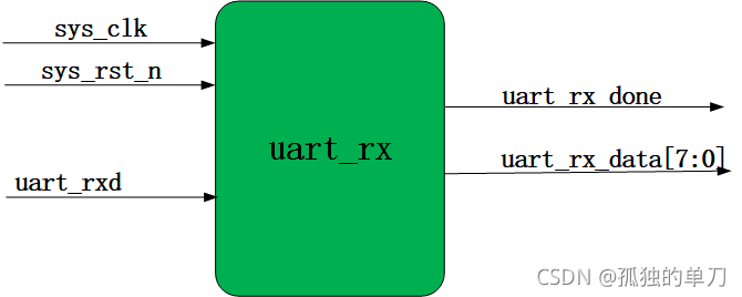
The overall block diagram of the reception module, along with input and output signals, is shown below:
The signal descriptions are as follows:
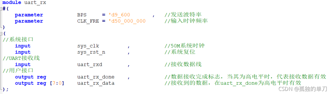
It should be noted that uart_rx_data is the byte of data received, and uart_rx_done is the reception completion flag. When it is pulled high, it indicates that the received serial data uart_rx_data is valid.
4.2 Design Concept
This module supports the reception of any baud rate (theoretically), but it needs to be instantiated with parameters when using this module, with 8 data bits, 1 start bit, and 1 stop bit, with no parity.
The transmission of the serial port starts with the start bit, which pulls the data line low, so we need to capture the falling edge of the data line and sample the receiving data line three times to capture its falling edge.
When the falling edge of the receiving data line is captured, the reception flag signal is pulled high, indicating that the module has entered the reception process; after receiving 10 bits, the reception flag signal is pulled low, indicating the end of the reception process.
Assuming a baud rate of 9600, the time to transmit one bit is 1s/9600, and a data transmission consists of 10 bits (8 data bits, 1 start bit, and 1 stop bit), thus requiring 1s/960 seconds in total.
Assuming the system clock is 50MHz (parameterized to adapt to different system frequencies), its period is 20ns, so the number of system cycles required to transmit one bit is (1s/960)/20ns ≈ 5208 cycles.
A counter is used during the reception process to count, with a range of (0~5208-1), which corresponds to 10 intervals (one byte requires receiving 10 bits);
Additionally, another counter is needed to count the number of bits received (each time the previous counter reaches 5207, it indicates that one bit has been received), with a range of (0~9).
During the reception process, based on the value of the counter (bit count), the received data is sampled and shifted into a register (data is most stable in the middle of the level).
If the bit count = 0, it indicates the start bit, and no data needs to be received;
If the bit count = 1, it indicates that the least significant bit (LSB) of the data needs to be received, and it is assigned to the lowest bit of the register;
······
If the bit count = 8, it indicates that the most significant bit (MSB) of the data needs to be received, and it is assigned to the highest bit of the register;
If the bit count = 9, it indicates the stop bit, and no data needs to be received.
4.3 Verilog Code
Based on the above design concept, part of the code is as follows:
// *******************************************************************************************************// ** Author : Lonely Sword // ** Email : [email protected]// ** Blog : https://blog.csdn.net/wuzhikaidetb // ** Date : 2022/08/05 // ** Function : 1. UART reception driver module based on FPGA; // 2. Configurable baud rate BPS, main clock CLK_FRE; // 3. 1 start bit, 8 data bits, 1 stop bit, no parity. // ******************************************************************************************************* module uart_rx#( parameter integer BPS = 9_600 , // Baud rate parameter integer CLK_FRE = 50_000_000 // Input clock frequency) ( // System interface input sys_clk , // 50M system clock input sys_rst_n , // System reset // UART receiving line input uart_rxd , // Receiving data line // User interface output reg uart_rx_done , // Data reception completion flag, when high, indicates that the received data is valid output reg [7:0] uart_rx_data // Received data, valid when uart_rx_done is high); assign neg_uart_rxd = uart_rx_d3 && (~uart_rx_d2); // Capture the falling edge of the data line to indicate the start of data transmission // Sample the data line three times to synchronize signals from different clock domains and prevent metastability always@(posedge sys_clk or negedge sys_rst_n)begin if(!sys_rst_n)begin uart_rx_d1 <= 1'b0; uart_rx_d2 <= 1'b0; uart_rx_d3 <= 1'b0; end else begin uart_rx_d1 <= uart_rxd; uart_rx_d2 <= uart_rx_d1; uart_rx_d3 <= uart_rx_d2; end end// After capturing the falling edge of the data (start bit 0), pull high the transmission start flag, and pull it low during the transmission of the 9th data (stop bit) to indicate the end of transmission always@(posedge sys_clk or negedge sys_rst_n)begin if(!sys_rst_n) rx_en <= 1'b0; else begin if(neg_uart_rxd ) rx_en <= 1'b1; // After receiving the 9th data (stop bit), pull the transmission start flag low to indicate the end of transmission, judging high level else if((bit_cnt == 4'd9) && (clk_cnt == BPS_CNT >> 1'b1) && (uart_rx_d3 == 1'b1) ) rx_en <= 1'b0; else rx_en <= rx_en; endend// When the data transmission reaches the stop bit, pull high the transmission completion flag and output the data always@(posedge sys_clk or negedge sys_rst_n)begin if(!sys_rst_n)begin uart_rx_done <= 1'b0; uart_rx_data <= 8'd0; end // After finishing reception, output the received data else if((bit_cnt == 4'd9) && (clk_cnt == BPS_CNT >> 1'd1) && (uart_rx_d3 == 1'b1))begin uart_rx_done <= 1'b1; // Pull high for one clock cycle uart_rx_data <= uart_rx_data_reg; end else begin uart_rx_done <= 1'b0; // Pull high for one clock cycle uart_rx_data <= uart_rx_data; endend // Every time a BPS_CNT (the number of clocks required to transmit one bit) is counted, increment the data counter by 1 and reset the clock counter always@(posedge sys_clk or negedge sys_rst_n)begin if(!sys_rst_n)begin bit_cnt <= 4'd0; clk_cnt <= 32'd0; end else if(rx_en)begin // In reception state if(clk_cnt < BPS_CNT - 1'b1)begin // A bit of data has not been received yet clk_cnt <= clk_cnt + 1'b1; // Clock counter +1 bit_cnt <= bit_cnt; // Bit counter remains unchanged end else begin // A bit of data has been received clk_cnt <= 32'd0; // Clear the clock counter, restart timing bit_cnt <= bit_cnt + 1'b1; // Bit counter +1, indicating that one bit of data has been received end end else begin // Not in reception state bit_cnt <= 4'd0; // Clear clk_cnt <= 32'd0; // Clear end end endmodule4.4 Testbench
The design of the simulation module’s Testbench is as follows:
Set the baud rate to 230400 (this is to facilitate observing the transmission enable signal uart_tx_en).
Define a task that will output one bit at a time using the baud rate of 230400, simulating the host sending data to the FPGA.
After 3000ns, send the first random data.
After sending the first random data, send the second random data, for a total of four random data transmissions.
// *******************************************************************************************************// ** Author : Lonely Sword // ** Email : [email protected]// ** Blog : https://blog.csdn.net/wuzhikaidetb // ** Date : 2022/07/29 // ** Function : 1. Testbench for the UART reception driver module based on FPGA // 2. Simulate the host timing to send data to the serial reception driver, observing whether the module can successfully receive data. // 3. Sequentially send 4 random 8-bit data // ******************************************************************************************************* `timescale 1ns/1ns // Define time scale // Module and interface definition module tb_uart_rx(); reg sys_clk ; reg sys_rst_n ; reg uart_rxd ; wire uart_rx_done ; wire [7:0] uart_rx_data ; localparam integer BPS = 'd230400 ; // Baud rate localparam integer CLK_FRE = 'd50_000_000 ; // System frequency 50M localparam integer CNT = 1000_000_000 / BPS ; // Calculate the time required to transmit each bit, in ns // Initial moment definition initial begin $timeformat(-9, 0, " ns", 10); // Define time display format sys_clk =1'b0; sys_rst_n <=1'b0; uart_rxd <=1'b1; #20 // System starts working sys_rst_n <=1'b1; #3000 rx_byte({$random} % 256); // Generate 8-bit random number 1 rx_byte({$random} % 256); // Generate 8-bit random number 2 rx_byte({$random} % 256); // Generate 8-bit random number 3 rx_byte({$random} % 256); // Generate 8-bit random number 4 #60 $finish();end // Every time a BYTE of data is successfully received, print it in the test window always @(posedge sys_clk)begin if(uart_rx_done)begin $display("@time%t", $time); $display("rx : 0x%h",uart_rx_data); endend // Define task, each sent data is 10 bits (1 start bit + 8 data bits + 1 stop bit) task rx_byte( input [7:0] data); integer i; // Define a constant // Use for loop to generate a frame of data, the last content in the for parentheses can only be written as i=i+1 for(i=0; i<10; i=i+1) begin case(i) 0: uart_rxd <= 1'b0; // Start bit 1: uart_rxd <= data[0]; // LSB 2: uart_rxd <= data[1]; 3: uart_rxd <= data[2]; 4: uart_rxd <= data[3]; 5: uart_rxd <= data[4]; 6: uart_rxd <= data[5]; 7: uart_rxd <= data[6]; 8: uart_rxd <= data[7]; // MSB 9: uart_rxd <= 1'b1; // Stop bit endcase #CNT; // Delay for each sent bit end endtask // End of task // Set main clock always #10 sys_clk <= ~sys_clk; // Clock 20ns, 50M // Instantiate the tested serial reception driver uart_rx#( .BPS (BPS ), .CLK_FRE (CLK_FRE ) )uart_rx_inst( .sys_clk (sys_clk ), .sys_rst_n (sys_rst_n ), .uart_rxd (uart_rxd ), .uart_rx_done (uart_rx_done ), .uart_rx_data (uart_rx_data ) ); endmodule4.5 Simulation Result Analysis
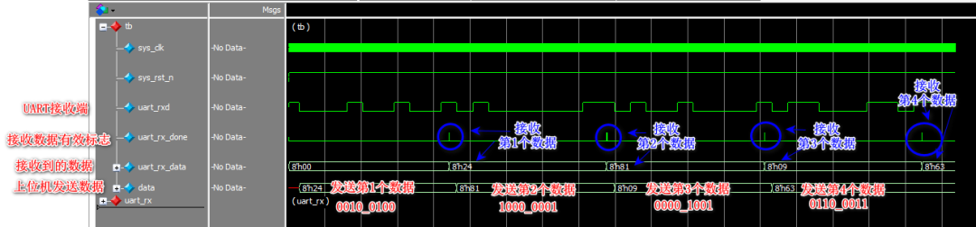
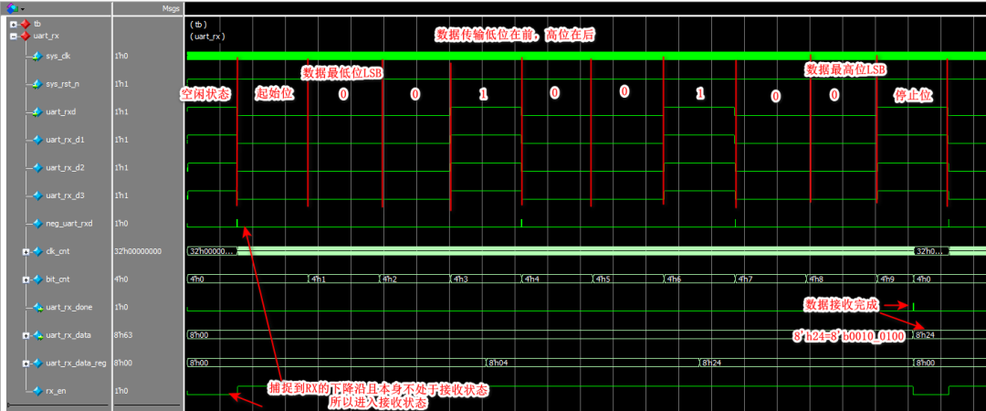
The simulation results are shown in the figure below (with detailed comments):
In the figure below, four data 8’h24–8’h81–8’h09–8’h63 were sent; the reception module received four data 8’h24–8’h81–8’h09–8’h63. The sent and received data are consistent.
Overall reception timing
The figure below shows the timing diagram for the first received data (8’h24, i.e., 00100100).
4.6 On-Board Testing
Having successfully completed the simulation verification of the reception module, the next step is to conduct on-board testing using an Altera Cyclone IV E development board.
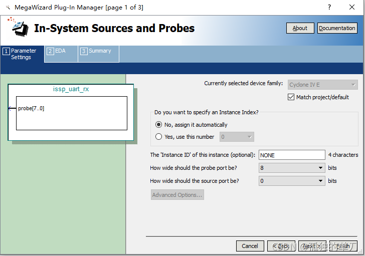
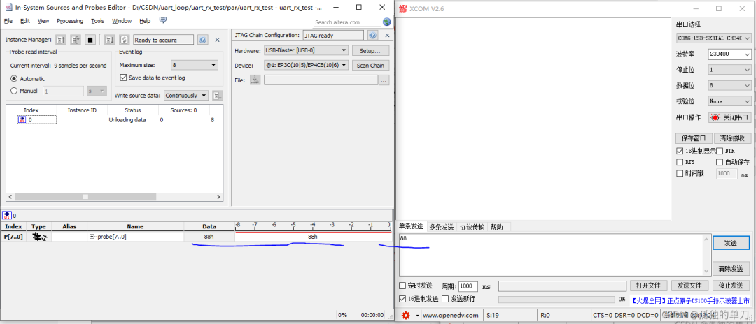
First, generate an IP core – ISSP (In-System Sources and Probes), which can provide an output for online output, equivalent to a simple signal generator – Source, and can also provide probes to monitor signal outputs online.
In this design, we use Probes to observe the data received by the serial port. The ISSP is called as follows:
A verification module for the reception module is written, which calls the reception module and the ISSP IP core. At the same time, a serial debugging software on the computer is used to send data, and the success of the serial reception module is determined based on the data received.
The verification module code for the reception module is as follows:
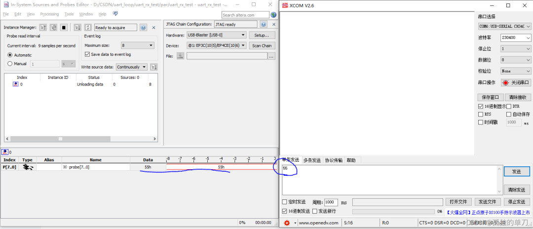
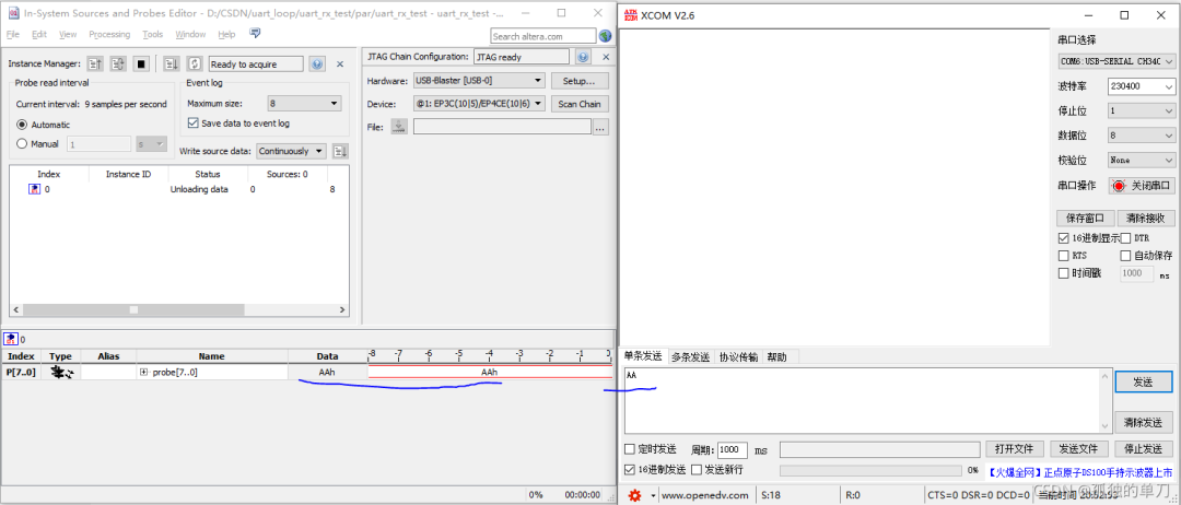
// *******************************************************************************************************// ** Author : Lonely Sword // ** Email : [email protected]// ** Blog : https://blog.csdn.net/wuzhikaidetb // ** Date : 2022/07/29 // ** Function : 1. Test module for the UART reception driver module based on FPGA; // 2. Instantiate the serial reception driver and ISSP IP core; // 3. Use the host to send random data to FPGA, and test by observing the data received by the reception driver monitored by ISSP. // ******************************************************************************************************* module uart_rx_test(// System interface input sys_clk , input sys_rst_n , // UART receiving line input uart_rxd // Receiving data line); parameter integer BPS = 'd230400 ; // Baud rate 230400 parameter integer CLK_FRE = 'd50_000_000 ; // System frequency 50MHZ wire [7:0] uart_rx_data; // Instantiate the reception module uart_rx#( .BPS (BPS ), .CLK_FRE (CLK_FRE )) uart_rx_isnt( .sys_clk (sys_clk ), .sys_rst_n (sys_rst_n ), .uart_rxd (uart_rxd ), .uart_rx_done ( ), .uart_rx_data (uart_rx_data ) ); // Instantiate ISSP as a monitoring tool issp_uart_rx issp_uart_rx_inst( .probe (uart_rx_data ), // Monitor received data .source ( ) ); endmoduleAfter downloading the program, open the In-System Sources and Probes Editor in Quartus II, and then use the serial debugging software to send data 0x55–0xaa–0x88 (three randomly selected values), observing the values of the registers in the In-System Sources and Probes Editor, which are as follows:
5. Conclusion
UART, as a commonly used communication protocol and debugging method, must be mastered proficiently!
Implementing UART based on FPGA is not difficult; as long as you pay attention to reasonably designing the counters according to the baud rate, data transmission and reception can be achieved under the control of these counters.
Copyright Statement: This article is an original article by CSDN blogger “Lonely Sword”, following the CC 4.0 BY-SA copyright agreement. Please include the original source link and this statement when reprinting.
Original link:
https://blog.csdn.net/wuzhikaidetb/article/details/114596930
「Share Hardware and Electronic Technology Essentials」」
Click👇 to follow, set as a star in the upper right menu···
「Recommended Reading 👇 Click the image to jump」
The principle, characteristics, and applications of hot-swappable technology
Using ADC to Accurately Measure Resistance Values
Support the author with a one-click three-way👉 Share↓ Like↓ View↓