Let’s explore the mysteries of DSP
To explore DSP
The DSP series main control chips are widely used in power electronics and switch-mode power supply circuits. Their powerful data computation and fixed-point floating-point processing capabilities make them extensively used for data acquisition and algorithm processing in circuits. Moreover, TI and ADI’s DSP chips come with a rich set of peripherals such as ADC, ePWM, eCAP, SCI, etc., greatly facilitating direct interaction with circuit data behavior.
This article takes the DSP28335-SCIA serial communication reception as an example to roughly explain the process of serial communication and interrupt implementation. Most tutorials on forums discuss the implementation before and after FIFO interrupts, but many bloggers have not noticed that there are two ways to implement serial reception interrupts:(Since there is only one entry for the SCIA reception interrupt in the interrupt vector table, both interrupt types share the same entry)
-
When a new byte of data enters SCIRXBUF, an interrupt request is generated;
-
When the FIFO TXFFIL storage depth equals the TXFFST set depth, a FIFO reception interrupt is generated.

1
Interrupt generated by SCIRXBUF data update
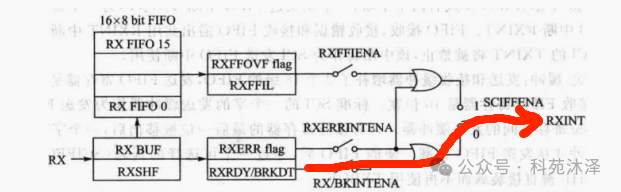
Figure 1 Interrupt generated by SCIRXBUF update
From the above Figure 1, it can be seen that the interrupt process generated by the SCI reception buffer register RXBUF involves the settings of three data bits: RXRDY or BRKDT, RX BKINTENA, and SCIFFENA. Next, we will look up the manual to find the register descriptions corresponding to these three data bits:
-
RXRDY is the SCI receive ready flag, located at bit 7 of the SCI receive status register SCIRXST. When new data can be read from the SCIRXBUF register, this bit is automatically set to 1. It is important to note that this bit is automatically cleared to 0 by hardware after reading the SCIRXBUF data, so there is no need to set it to 0 in software.

Figure 2 Description of SCIRXBUF.RXRDY data bit
//RXBUF receive interrupt, when new data enters, RXRDY is set to 1;SciaRegs.SCIRXST.bit.RXRDY = 0;//Mask FIFO receive interrupt, not using FIFO;SciaRegs.SCIFFRX.all=0x6040; Settings: Mask FIFO receive enable, while enabling RXRDY bit


2.RX/BK INT ENA is the SCI receive buffer/suppress interrupt enable flag, located at bit 1 of SCI control register 2-SCICTL2. The function of this bit is to enable the receive or error interrupt bit in conjunction with interrupts triggered by RXRDY or BRKDT.

Figure 3 Description of SCICTL2.RXBKINTENA data bit
//Enable SCI receive buffer/suppress interrupt set to 1SciaRegs.SCICTL2.bit.RXBKINTENA =1;Settings: Enable RXBKINTENA interrupt flag
3.SCIFFENA is the SCI interrupt mode selection register flag, located at bit 14 of the SCI transmit FIFO register SCIFFTX. Its function is to select the interrupt mode. When this bit is set to 0, it masks the RXBUF update interrupt mode and selects the FIFO receive interrupt; when this bit is set to 1, it masks the FIFO receive interrupt and selects the RXBUF update interrupt mode. Note: When this bit is 0, both FIFO send and receive functions cannot be used.

Figure 4 Description of SCIFFTX.SCIFFENA data bit
//Mask SCI FIFO functionSciaRegs.SCIFFTX.bit.SCIFFENA = 0;Settings: Data reception interrupt mode selection code snippet
Conclusion
The RXBUF update interrupt mode is essentially triggered by the update of new data in RXBUF, so each interrupt can only receive one byte of data, making its efficiency extremely low compared to the FIFO receive interrupt mode, and its flexibility is also very limited. It is generally only used for testing or receiving small amounts of data.
/********** RXBUF update receive interrupt **********/__interrupt void sciaRxBufIsr(void){ if(SciaRegs.SCIRXST.bit.RXRDY == 1) { // Get character ReceivedChar = SciaRegs.SCIRXBUF.all; } msg = " You sent: "; UARTa_SendString(msg); UARTa_SendByte(ReceivedChar); SciaRegs.SCIFFRX.bit.RXFFINTCLR=1; // Clear Interrupt flag PieCtrlRegs.PIEACK.all|=0x100; // Issue PIE ack}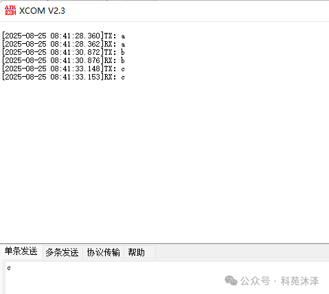
Figure 5 Display of RXBUF data update interrupt mode reception
2
FIFO reception overflow or full frame interrupt mode
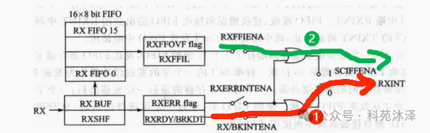
Figure 6 FIFO reception overflow or full frame interrupt mode process
From the above Figure 5, it can be seen that the interrupt process generated by the SCI-FIFO reception interrupt mode involves the settings of three data bits: RXFFOVF or RXFFIL, RX FFIENA, and SCIFFENA. Next, we will look up the manual to find the register descriptions corresponding to these three data bits:
-
RXFFOVF and RXFFIL are both SCI receive FIFO register flag bits, located at bit 15 and bits 0-4 of the SCI receive FIFO register SCIFFRX. In FIFO receive mode, when the RXFFOVF overflow flag is set to 1, it indicates that the FIFO has filled 16 bytes of data and is about to overflow, at which point a FIFO interrupt signal will be generated. Additionally, when the number of bytes stored in RXFFIL bits 0-4 equals the number of bytes set in RXFFST bits 0-4, a FIFO interrupt signal will also be generated. These two interrupt signals are the green interrupt signals in the above Figure 6.Line.
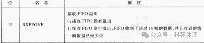
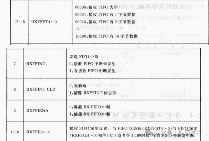
Figure 7 Description of RXFFOVF and RXFFIL register data bits
//Set RXFFOVF overflow bit initialization to 0 for no overflow;//Set RXFFST0~4 depth data bits to FIFO_SIZE size, when RXFFIL stores FIFO_SIZE bytes, trigger interruptSciaRegs.SCIFFRX.all=0x6060 | FIFO_SIZE;Settings: Overflow flag bit and depth data bit configuration
2. RXFFIENA is the SCI receive FIFO register flag bit, located at bit 5 of SCIFFRX. When this bit is set to 1, it indicates that the RX FIFO interrupt is enabled. It only needs to be initialized once during the configuration process, and there is no need to repeat the configuration afterwards.

Figure 8 Description of RXFFIENA register data bit
//Enable FIFO receive interruptSciaRegs.SCIFFTX.bit.RXFFIENA = 1;Code snippet: Enable FIFO receive interrupt
3. SCIFFENA is the SCI interrupt mode selection register flag, located at bit 14 of the SCI transmit FIFO register SCIFFTX. Its function is to select the interrupt mode. When this bit is set to 0, it masks the RXBUF update interrupt mode and selects the FIFO receive interrupt; when this bit is set to 1, it masks the FIFO receive interrupt and selects the RXBUF update interrupt mode. Note: When this bit is 0, both FIFO send and receive functions cannot be used.
Figure 9 Description of SCIFFTX.SCIFFENA data bit
//Enable SCI FIFO functionSciaRegs.SCIFFTX.bit.SCIFFENA = 1;Settings: Data reception interrupt mode selection for FIFO mode interrupt
Conclusion
Compared to the RXBUF interrupt, the FIFO receive interrupt mode is very flexible, allowing for custom interrupt byte depth settings and includes built-in FIFO overflow interrupt monitoring. The terminal frequency can be set through programming, and its usage is quite widespread, primarily used in industrial RS232 and RS485 control communications. It is important to note that after entering the interrupt, the FIFO interrupt flag must be manually cleared to ensure that the next interrupt can be entered. In actual communication, the FIFO interrupt mode is generally recommended for use.
/********** FIFO receive interrupt **********/__interrupt void sciaRxFifoIsr(void){ msg = "\r\nReceive 8 Byte data already!\r\n"; UARTa_SendString(msg); Uint16 i; if(SciaRegs.SCIRXST.bit.RXERROR == 0){ for(i=0;i<SET_FIFO_SIZE;i++) { rdataA[i]=SciaRegs.SCIRXBUF.all; // Read data ASCII code + 1 } } rdataA[SET_FIFO_SIZE] = '\0';//Null-terminated to avoid garbled symbols from FIFO RXBUF overflow UARTa_SendString(rdataA); SciaRegs.SCIFFRX.bit.RXFFOVRCLR=1; // Clear Overflow flag SciaRegs.SCIFFRX.bit.RXFFINTCLR=1; // Clear Interrupt flag PieCtrlRegs.PIEACK.all|=0x100; // Issue PIE ack}Code snippet: FIFO receive interrupt function configuration
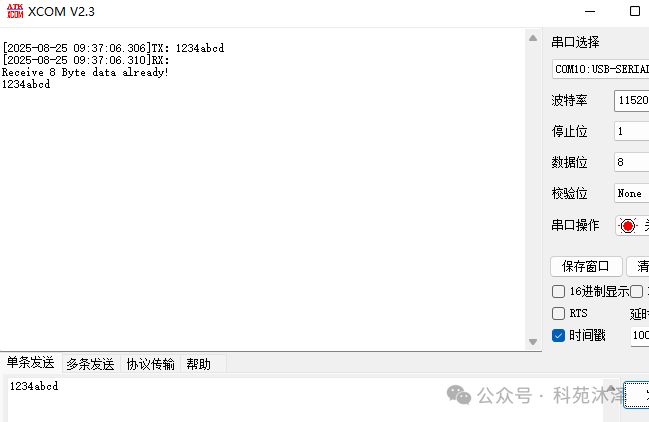
Figure 10 8-byte depth FIFO receive interrupt data transmission
—— E N D ——
Text: From Muze
Cover and illustrations: Muze
Long
Press
Close
Note
Science Garden Muze
ID : keYuanMuze
Searching for light in life…..