In the ASIC market, some recent statements heard are contradictory.
“Among the many ASIC projects globally, 90% will fail,” said NVIDIA CEO Jensen Huang.
Huang’s comments on ASIC are not frequent. Therefore, once the related remarks were made, discussions about the growth potential of ASIC surged in the market, with various speculations emerging.
Huang stated that compared to NVIDIA’s focus on general-purpose GPU architecture, ASIC is designed for specific tasks. While it excels in performance and efficiency for single-use cases, it lacks flexibility and scalability. This “single-point optimization” strategy struggles to cope with the rapid evolution of AI applications. Huang’s evaluation of ASIC does not deny its value but emphasizes that “the entry barrier and operational difficulty are very high.” He cited Google’s TPU as an example, stating that its team is the “strongest ASIC team in the world,” yet even so, Google’s Gemini model is still deployed on NVIDIA’s GPU as well.
However, there is another voice in the market that is equally justified— in the rapid development of ASIC, NVIDIA has sensed the danger signals.
 01Can ASIC Surpass GPU?
In the computing chip market, there are quite a few “supporters” of ASIC chips. With the push from major ASIC chip manufacturers and cloud giants, the AI computing market is approaching a new critical point.
According to a recent report from Nomura Securities, NVIDIA’s GPU currently occupies over 80% of the AI server market, while ASIC only accounts for 8%-11%.
However, from the perspective of shipment volume, the situation is changing. By 2025, Google’s TPU shipment is expected to reach 1.5-2 million, while Amazon’s AWS Trainium 2 ASIC is about 1.4-1.5 million, and NVIDIA’s AI GPU supply will exceed 5-6 million.
Supply chain investigations show that the total shipment of Google and AWS’s AI TPU/ASIC has already reached 40%-60% of NVIDIA’s AI GPU shipment.
As Meta plans to start large-scale deployment of its self-developed ASIC solutions in 2026, and Microsoft will begin large-scale deployment in 2027, it is expected that the total shipment of ASIC will surpass NVIDIA’s GPU shipment at some point in 2026.
This also means that the era of ASIC will officially arrive.
The news that OpenAI announced testing Google’s TPU has further ignited market enthusiasm. It is reported that the AI technology giant OpenAI has begun renting Google’s AI chips to support the computing needs of its ChatGPT and other products. In response, OpenAI stated that there are currently no plans to use Google’s self-developed chips to drive its products.
However, an OpenAI spokesperson pointed out that while the company’s AI lab is indeed in the preliminary testing of some of Google’s TPU, there are currently no plans for large-scale adoption.
Currently, OpenAI mainly relies on NVIDIA’s GPU and AMD’s AI chips to meet its growing AI computing needs. To reduce dependence on NVIDIA and AMD, OpenAI is also developing its own chips, planning to achieve the “tape-out” milestone this year, which means the chip design is complete and sent for manufacturing.
The last company to cause a stir by using Google’s TPU was Apple. Last July, Apple disclosed in a paper on its official website that its training model used Google’s fourth-generation AI ASIC chip TPUv4 and the newer generation chip TPUv5.
Before last year, compared to NVIDIA’s GPU, Google’s TPU seemed like an “unknown” rookie, but now it appears to have the strength to compete with NVIDIA’s GPU.
However, in my opinion, “Will ASIC chips be able to crush GPUs in the future?” This seems more like a false proposition.
02ASIC, Core Advantages
The market generally believes that ASIC chips are becoming an important branch of AI chips. However, what specific advantages does ASIC have to impact GPU? And what specific impacts are there? There is relatively little discussion on this.
In response to a series of questions, I will discuss this.
According to different tasks, AI chips can mainly be divided into two categories: AI training chips and AI inference chips.
By 2025, the global demand for AI inference computing power is expected to explode, especially in edge application scenarios. This is also an opportunity for ASIC.
First, let’s talk about what inference is.
Inference is the process of “processing data with a trained model” (for example, using a trained image recognition model to identify photos, or using a speech model to transcribe speech). Once a model is deployed, its algorithm logic (such as the convolutional layers of CNN, the attention mechanism of Transformer) and computational flow (input-output format, precision requirements) will be fixed for a long time, requiring almost no adjustments.
This “fixedness” perfectly matches ASIC‘s core advantage— custom hardware architecture for single tasks: it can directly “solidify” the computational logic and data paths of inference algorithms into the chip, removing all irrelevant general computing units (such as the dynamic scheduling modules and general memory controllers used for training in GPU), allowing hardware resources to serve 100% for inference computing.
Similarly, ASIC has relatively weaker capabilities in training tasks. Because training task algorithms iterate quickly and require flexibility. If an ASIC is used for training, when the algorithm updates, the chip faces the risk of obsolescence, and the cost-effectiveness is much lower.
Inference scenarios are far more sensitive to “energy efficiency ratio” (the computing power provided per watt of power) and “cost” than training. In these two aspects, ASIC has a crushing advantage.
In terms of energy efficiency ratio, Google’s TPU v5e has an energy efficiency ratio three times that of NVIDIA’s H100.
In terms of cost,AWS‘s Trainium 2 has a cost-effectiveness ratio in inference tasks that is 30%-40% higher than that of H100, and Google’s TPUv5 and Amazon’s Trainium2 unit computing cost is only 70% and 60% of NVIDIA’s H100.
A large model may only require dozens to hundreds of training chips (such as GPU), but the inference phase may require tens of thousands or even hundreds of thousands of chips (for example, the inference cluster scale of ChatGPT is more than ten times that of the training cluster). Therefore, the “customization” design of ASIC can reduce the cost per chip.
VerifiedMarketResearch data shows that the market size of AI inference chips was 15.8 billion USD in 2023, and it is expected to reach 90.6 billion USD by 2030, with a compound annual growth rate of 22.6% during the forecast period from 2024 to 2030.
Stay tuned and bookmark eFocus for industry insights.
Scan to reply with the keyword “GPU“ for industry groups and to receive reports.
Currently, the inference scenario is presenting a pattern of coexistence and competition between ASIC and GPU, with a huge market space for ASIC chips.
Recently, Broadcom’s CEO Hock Tan and CFO Kirsten Spears also emphasized in a meeting that the company’s orders in the AI inference field have significantly increased, and the company is currently working closely with four potential AI XPU customers, planning to complete the first generation of AI XPU products for major clients such as Arm/SoftBank and OpenAI this year.
Now let’s look at the competitive landscape in the training market.In the AI training chip market, there are hardly any competitors, with NVIDIA alone occupying over 90% of the AI training market share, supporting the training of 18 trillion parameter models with its Blackwell architecture, and achieving seamless interconnection of 72-card clusters through NVLink 6 technology.
As mentioned above, the “flexibility” of training tasks naturally aligns with the GPU architecture, and in addition, NVIDIA has built an unshakeable software ecosystem through the CUDA platform: over 90% of AI frameworks (TensorFlow, PyTorch) natively support CUDA, allowing developers to call on GPU computing power without rewriting code. This ecological inertia means that even if manufacturers like AMD and Huawei launch training chips with comparable performance, the user migration cost remains extremely high.
Industry insiders have told Semiconductor Industry Review that the stability of model architecture is the core premise for ASIC to realize its value—when the model is stable, the low cost and high efficiency advantages of ASIC can be fully released; when the model iterates quickly or even undergoes revolutionary changes, ASIC is prone to obsolescence due to adaptation lag.
This is also why some industry experts point to 2026 as the node for the explosion of the ASIC market scale. The design cycle of ASIC can take 1-2 years, while the iteration speed of AI models is extremely fast (for example, the large model from GPT-3 to GPT-4 took only one year). If the model that the ASIC design is anchored to becomes outdated (for example, if Transformer replaces CNN), the chip may become directly obsolete.
Now, with the development of large models, algorithms are initially solidified. Coupled with the continuous decline in the cost of ASIC, it has a better stage to showcase itself.
As for whether ASIC will replace GPU? In my opinion, this question is premature.
In the short term, the competition between ASIC and GPU is essentially a trade-off between “efficiency” and “flexibility”; the two are not currently in a mutually exclusive relationship. The advantages of ASIC in specific scenarios cannot break the ecological barriers of GPU; while the generality of GPU makes it difficult to replace in complex tasks. In the future, both will achieve optimal resource allocation through hybrid architectures (such as GPU + ASIC accelerator cards) and heterogeneous computing (such as CUDA and custom instruction sets working together).
As the AI market develops, what kind of chips will be needed remains to be seen.
03Chip Leaders Enter ASIC
In addition to Google, many AI chip companies both domestically and internationally are choosing to embrace ASIC.
Meta
Meta’s core computing load comes from recommendation system scenarios, providing a fertile ground for self-developed, specialized ASIC chips.
Meta launched the MTIA V1 and MTIA V2 chips in 2023 and 2024, respectively. In addition, Meta plans to launch the MTIA V3 chip in 2026, which is expected to be equipped with high-end HBM, and unlike the V1/V2 chips that focus on specific tasks such as advertising and social networking, it is expected to expand applications to model training and inference tasks.
AmazonAWS
AWS has laid out its AI chip strategy mainly around inference chips Inferentia and training chips Trainium.
Since 2020, Amazon has released three generations of Trainium chips. Among them, Trainium3 is expected to improve performance by two times compared to the previous generation, with a 40% increase in energy efficiency, and the performance of UltraServers equipped with this chip is expected to increase fourfold.
Microsoft
In November 2023, Microsoft released its first self-developed AI chip, Azure Maia 100, at the Ignite technology conference, as well as a chip for cloud software services, Azure Cobalt. Both chips will be manufactured by TSMC using 5nm process technology.
Cobalt is a general-purpose chip based on the Arm architecture, featuring 128 cores, while Maia 100 is an ASIC chip designed specifically for Azure cloud services and AI workloads, with a transistor count reaching 105 billion. These two chips will be integrated into Microsoft’s Azure data centers to support services such as OpenAI, Copilot and others.
The design of the next-generation Maia v2 has been confirmed, with backend design and mass production delivery handled by GUC. In addition to deepening cooperation with GUC, Microsoft has also involved MediaTek in the design development of the advanced version of Maia to strengthen its self-developed chip technology layout and effectively disperse technical and supply chain risks during the development process.
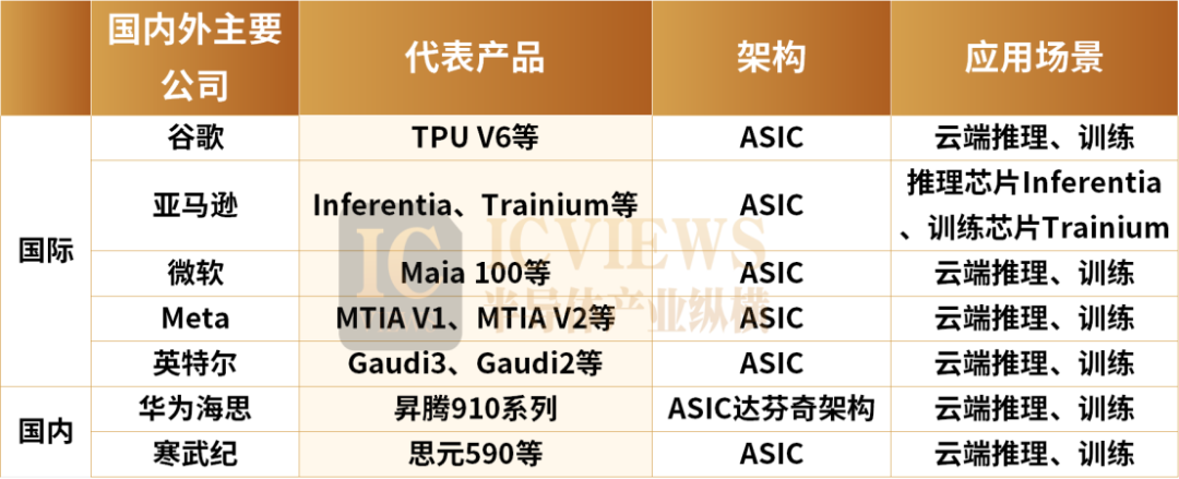
In China, the performance of ASIC chips is outstanding, particularly from Huawei and Cambricon.
Huawei’s Ascend series processors have achieved significant breakthroughs in both technology and application since their inception, especially the Ascend 910B.
Cambricon, as a leader in the domestic AI chip design field, is increasingly competitive in inference computing and AI acceleration for edge devices. Cambricon’s flagship product, MLU590, focuses on AI training and inference.
In the global AI chip competition, domestic ASIC chips face challenges but also historic opportunities. Through continuous innovation and technological breakthroughs, domestic ASIC is gradually expanding its market share.
04Two Beneficiaries of ASIC Chips
In the ASIC market, Broadcom currently ranks first with a share of 55% to 60%, while Marvell ranks second with a share of 13% to 15%.
Broadcom’s core advantage in the AI chip field lies in customized ASIC chips and high-speed data exchange chips, with solutions widely used in data centers, cloud computing, HPC (high-performance computing), and 5G infrastructure. Broadcom’s ASIC chip business has become its core growth point. Financial reports reveal that sales of customized AI chips (ASIC) are expected to account for 70% of total AI semiconductor revenue in the second quarter, reaching 30.8 billion USD (approximately 45 billion USD).
Currently, Broadcom has partnered with three hyperscale cloud service providers (such as Google, Meta, and ByteDance) and has added clients such as OpenAI and Apple, with plans to expand to seven large tech companies in the future. Among them, Broadcom has two major collaborations that are particularly noteworthy: the first is that Meta and Broadcom have collaborated to develop the first two generations of AI training acceleration processors, and both parties are currently accelerating the development of the third generation MTIA chip, which is expected to make significant progress in the second half of 2024 to 2025.
Marvell’s customized ASIC business is becoming one of its core growth drivers. In Marvell’s specific business, the data center business accounts for about 75%, which is a high-growth business. This part of the business includes SSD controllers, high-end Ethernet switches (Innovium), and customized ASIC business (customized chips for Amazon AWS), mainly applied in cloud servers, edge computing, and other scenarios.
Based on company communications and industry chain information, it is speculated that Marvell’s current ASIC revenue mainly comes from Amazon’s Trainium 2 and Google’s Axion Arm CPU processors, and the company’s Inferential ASIC project in collaboration with Amazon is expected to begin mass production in 2025 (i.e., the 2026 fiscal year). The project with Microsoft, Microsoft Maia, is expected to be completed in 2026 (i.e., the 2027 fiscal year).
END
Note: The cover image of this article is from freepik, self-made by the author, and publicly available media, all authorized.
Industry Community