In the field of electronic engineering, reverse engineering existing PCB boards is a common practice for many engineers or companies. This practice, known as “peeling apart,” is an important step for understanding circuit design, troubleshooting, or reproducing designs. So how can we efficiently peel apart a PCB board?
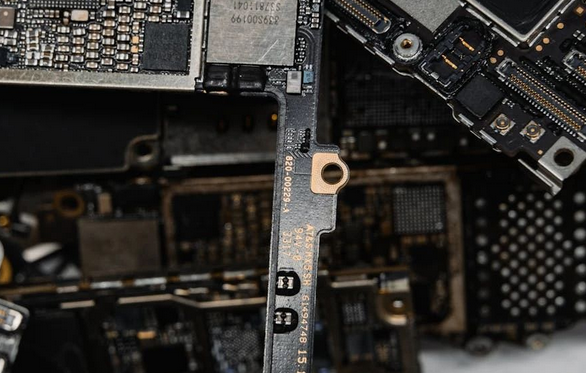
1. Record Component Information
Carefully record the model, parameters, and specific locations of all components on the PCB.
Make special notes of the orientation of diodes, transistors, and the notch direction of IC chips.
Use a digital camera to take layout photos of the components for future reference.
2. Component Removal and Cleaning
Remove all components and clear the solder from the PAD holes.
Thoroughly clean the PCB with alcohol to ensure no residues remain on the surface.
3. Scan the Silkscreen Layer
Place the cleaned PCB into a scanner and use software like Photoshop to scan the silkscreen side in color mode, then print it out.
4. Sand and Scan the Copper Layer
Lightly sand the top layer (TOP LAYER) and bottom layer (BOTTOM LAYER) of the PCB with fine sandpaper until the copper film shines.
Scan both layers separately, ensuring the PCB is flat in the scanner to avoid image distortion.
5. Image Processing
In Photoshop, adjust the image contrast and brightness to enhance the contrast between copper and non-copper areas.
Convert the image to black and white, and check the clarity of the lines, repeating the sanding and scanning steps if necessary.
Save as BMP format files (TOP.BMP and BOT.BMP).
6. Convert to Protel Format
Convert the BMP files to a format recognizable by PROTEL software and import them into PROTEL.
Compare the positions of the PADs and VIAs on both layers to ensure precise alignment.
7. Draw the PCB Diagram
Convert the TOP.BMP and BOT.BMP to PROTEL’s SILK layer (yellow layer) and manually trace the lines.
Place the components according to the original records, and delete the SILK layer upon completion.
8. Merge Layers
In PROTEL, merge the PCB diagrams of the TOP and BOT layers into a complete PCB design file.
9. Verification and Output
Use a laser printer to print the TOP and BOTTOM layers at a 1:1 ratio onto transparent film.
Overlay the film on the original PCB for comparison and verification to ensure accuracy.
This article is an original piece by FanYi Education. Please cite the source when reprinting!