Simply completing the simulation SPI implementation for various interfaces is obviously not enough just by capturing the signal timing with an oscilloscope.
Although the signal output by the microcontroller as the SPI master is easy to capture, the data sent by the slave (i.e., the timing of the master reading the MISO signal) requires finding a SPI peripheral device. This way, the master sends data, and the slave responds. For example, using SPI-FLASH, we found a W25Q16 FLASH to verify the correctness of communication between the simulated SPI interface and the FLASH device.
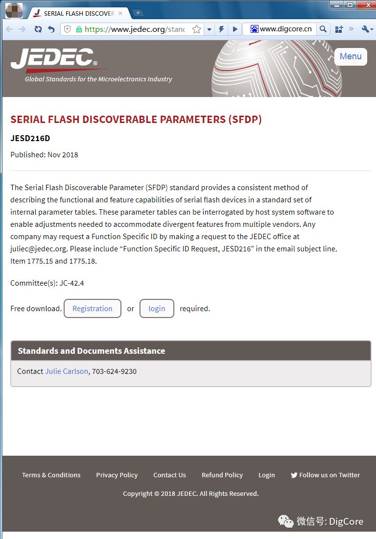
To proficiently use W25Q16, one must invest effort in learning the Spec; to master SPI-FLASH, it is even more important to understand the JEDEC organization’s SFDP (Serial Flash Discoverable Parameters, a specification for serial flash discoverable parameters). The official link is:
https://www.jedec.org/standards-documents/docs/jesd216b
Foreign websites load slowly, so here’s a screenshot:
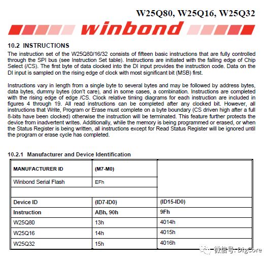
From the W25Q16 manual, various interfaces can be checked. To verify the correctness of SPI communication, we first perform the simplest read of the JEDEC specification-defined chip ID command (0x9F).
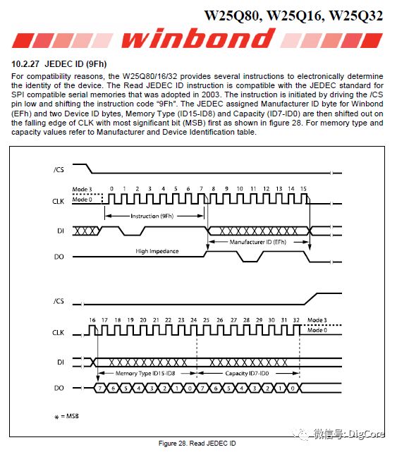
Based on the timing diagram of the JEDEC ID (9Fh) command, we use the implemented SPI interface in the program to send commands and receive data. This command can be used to verify the correctness of the data sent and received by the simulated SPI interface.
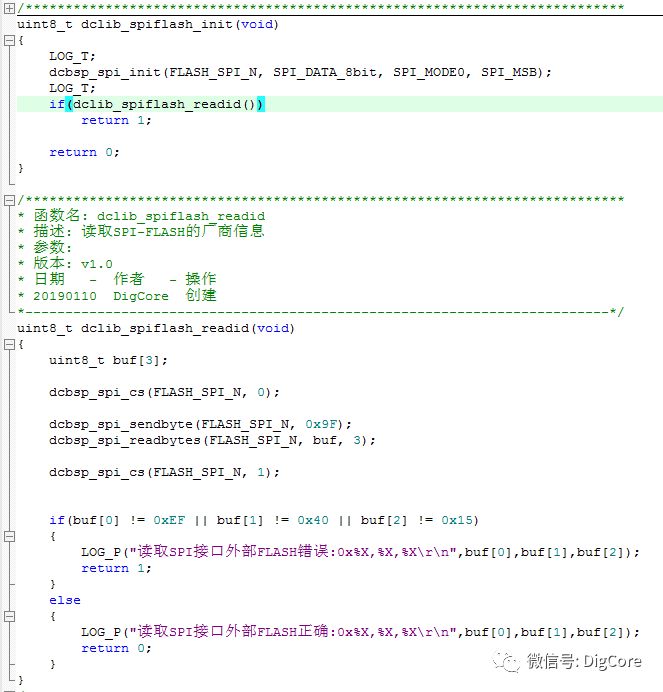
For readers who have seen the previous article “Embedded Hardware Communication Interface Protocol-SPI (II) Layered Architecture Design of the Simulated Interface,” I will briefly explain the code. Compared to the source code mentioned in the previous article, this time I made a modification to the function interface for reading one byte of data:
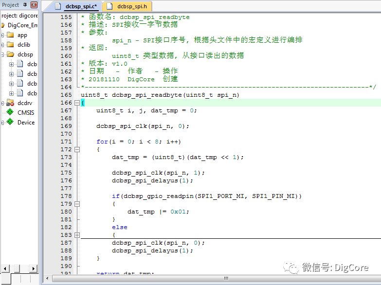
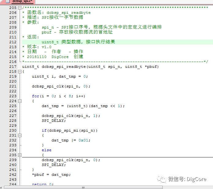
The modified approach is to pass the address as a parameter, storing the read data at that address, allowing the return value of the interface to indicate whether the interface executed correctly.
This consideration is mainly for portability across different platforms. If using hardware SPI interfaces, some hardware SPI interfaces may use a while loop to wait on registers, so timeout situations need to be considered. Therefore, it is necessary to reserve a return value as the function execution result, while the actual data read is placed in the space pointed to by the passed address parameter.
To verify the correctness of the simulated SPI interface, we read the vendor ID of the SPI-FLASH chip and check if the data read matches the manual.
The FLASH functional module belongs to the module library layer, situated between the application layer and the driver layer. Thus, the source code for the SPI-FLASH module is encapsulated into the lib layer.
Create source files:
dclib_spiflash.c
dclib_spiflash.h
Similarly, the FLASH design also needs initialization, which requires calling the BSP layer’s simulated SPI interface initialization, setting the SPI communication configuration items to match the FLASH chip: data width, clock polarity (CPOL), clock phase (CPHA), and data bit endianness selection.
After completing the SPI initialization, directly initiate communication with the FLASH device. The simplest command (0x9F) can read the FLASH chip’s vendor ID.
Burn the program into the microcontroller and check the reading effect to preliminarily verify the correctness of communication.
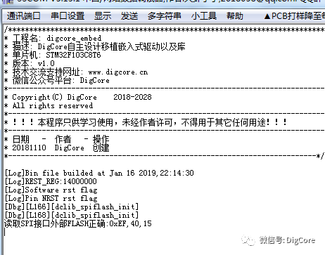
Comparing with the manual’s description, the read JEDEC ID is completely consistent with the manual.
Thus, it can be confirmed that the GPIO-simulated SPI interface can communicate correctly.
For more operations regarding SPI-FLASH, one should carefully read the data manual. If you need reference implementation source code, you can search for related source code on open-source platforms.
★★★★★ Recommended Articles
“【Embedded Programming】Function Return Type Design”
“【Embedded Programming】Solutions for Platform Endianness Storage Differences”
“Embedded Hardware Communication Interface – Using RingBuffer to Handle Data (II) Detailed Design Process”
“Embedded Hardware Communication Interface – Using RingBuffer to Handle Data (I)”
“Rapid Development of MQTT (I) MQTT from the Perspective of Electronic Engineers”
“Rapid Development of MQTT (II) Introduction to MQTT”
“Building MQTT Client – The Clearest MQTT Protocol Architecture”
“Building MQTT Server – The Fastest Way to Validate Your Developed Client”
★★★★★ Similar Articles
“Embedded Hardware Communication Interface Protocol – UART (V) Packet Design and Parsing”
“Embedded Hardware Communication Interface Protocol – UART (IV) Design of Start and Stop Style Application Layer Protocol”
“Embedded Hardware Communication Interface Protocol – UART (III) Quick Use of Serial Port and Applications”
“Embedded Hardware Communication Interface Protocol – UART (II) Standards Under Different Electrical Specifications”
“Embedded Hardware Communication Interface Protocol – UART (I) Protocol Basics”
“Embedded Hardware Communication Interface Protocol – SPI (II) Layered Architecture Design of Simulated Interfaces”
“Embedded Hardware Communication Interface Protocol – SPI (I) Protocol Basics”
★★★★★ Further Reading
“【Hardware Circuit】 AltiumDesigner18 Rule Check Meaning”
“【Hardware Circuit】 Basic Principles and Application Cases of N-channel and P-channel MOSFETs”

Long press the QR code to followDigCore
Follow the public account, send a message:
Download&dcbsp_spi
Get this articlePDF OriginalorSource CodeDownload Link


www.digcore.cn
More technical insights await you
Long press the QR code to follow