If you don’t want to miss my updates, remember to check the public account in the upper right corner and mark it as a star, take down the star and give it to me.

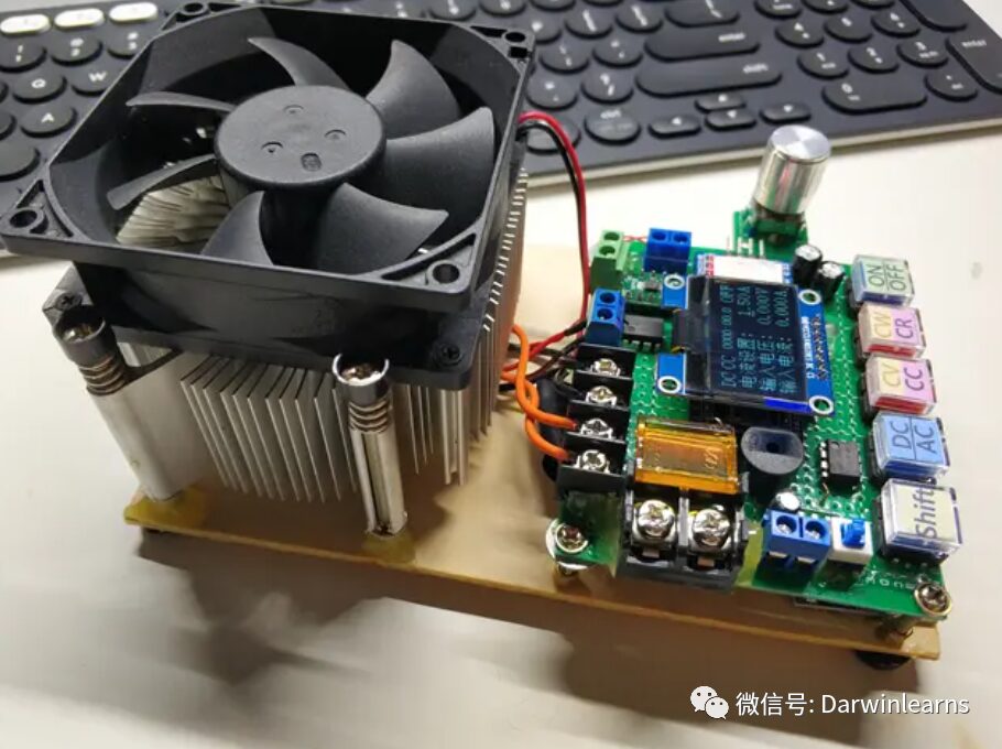
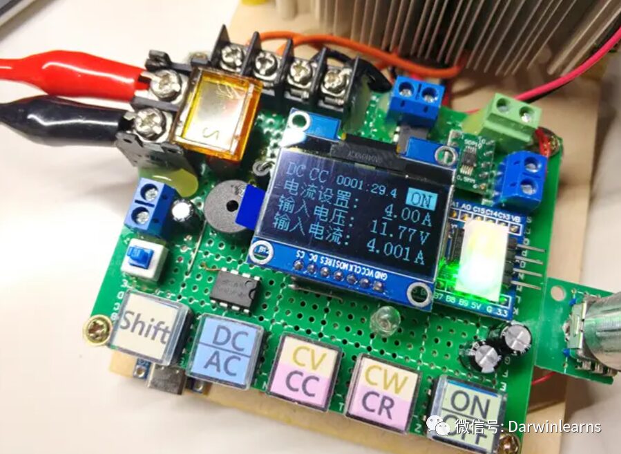
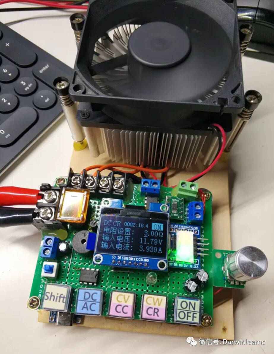
The project I am sharing today is a simple electronic load designed by Yu Hao based on STM32 control, featuring constant current, constant voltage, constant resistance, and constant power functions, with a maximum input voltage of 100V, thermal design power of 100W, and a maximum load current of 12A.
System Structure Diagram
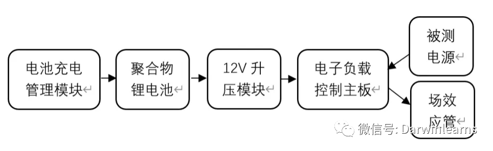
System Structure Block Diagram
Hardware Design
This module uses two IRFP250 field-effect transistors as the load transistors for the electronic load. P1 is the power input interface of the tested power source, R3 and R4 are the current detection sampling resistors, and the current detection amplifier uses the INA180A3 device, which has a voltage gain of 100V/V and an input offset voltage of 25uV.
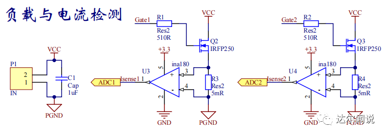
Load and Current Detection Schematic
Design considerations:
1) R1 and R2 are necessary and their resistance values cannot be too small; if the resistance is too small, it may cause the operational amplifier output voltage to oscillate at high frequencies, affecting circuit operation. The resistance values should be selected based on the output characteristics of the operational amplifier.
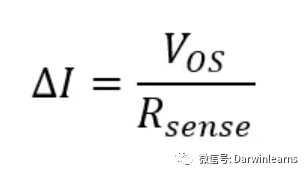
Using INA180A3 as the current detection amplifier, the offset current is about 5mA, while using LM358 to form a non-inverting proportional amplifier would yield an offset current of 100mA. To further reduce the offset current, the voltage gain can be reduced and the sampling resistance increased.
3) The accuracy and stability of the current detection resistor also directly affect the measurement accuracy. It is best to use a high-stability metal film resistor or constantan wire as the current sampling resistor.
✔ Load Transistor and Current Detection
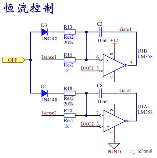
Constant Current Control Circuit
1) C3, C8, R16, and R20 form an inverting proportional integrator to limit the rise and fall rate of the operational amplifier output, suppressing overshoot or oscillation. If the current overshoot is too large, the capacitance of the integrator can be appropriately increased, but this will reduce the response speed of the circuit.
2) Due to the influence of the amplifier’s offset voltage and the offset of the DAC’s zero point, it may cause the load current not to be zero (about several milliamps of leakage current) when the DAC outputs a voltage of 0, making it impossible to turn off the electronic load by only outputting 0 voltage from the DAC. Therefore, a simple voltage raising circuit is added using D3, D1, R13, and R18; when the electronic load needs to be turned off, a high level can be output through the “OFF” network while the DAC outputs 0 voltage to completely turn off the field-effect transistor.
Current issues and improvement methods:
When the current supplied by the power source cannot reach the set current value, LM358 will output a high level (about 11V), and the field-effect transistor enters the variable resistor region. Excessive gate charge accumulation can cause the transistor to switch back to the constant current region too slowly. This can be improved by lowering the supply voltage of LM358 (to about 7V) to limit its output voltage amplitude.
✔Input Voltage Detection Circuit
Voltage Detection Circuit
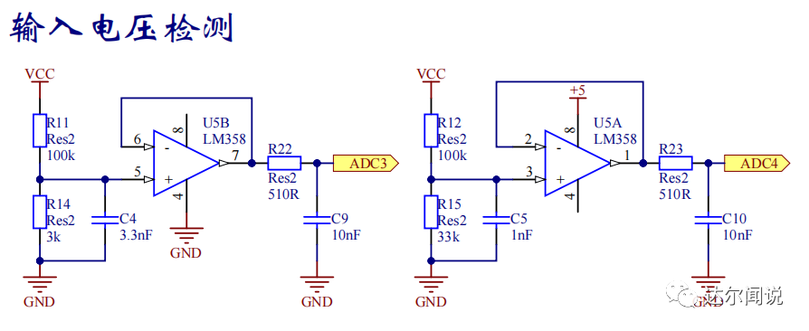
1) Due to the small input resistance of the integrated ADC of STM32 (the manual data is 50kΩ, and the shorter the sampling time, the smaller the input impedance), directly using the resistor divider method to sample the input voltage will lead to significant measurement errors. Therefore, an operational amplifier is used as the input buffer for the ADC.
2) The instantaneous input resistance of STM32’s ADC is very small, so it is recommended to add a buffer capacitor at the ADC pin. R22 and R23 serve to prevent oscillation of the operational amplifier.
3) Two different voltage ranges can be set separately to improve the voltage measurement accuracy at low voltages.
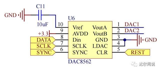
DAC8562 Schematic
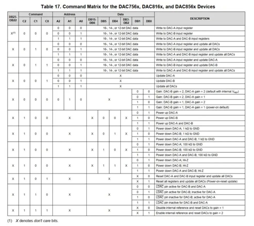
DAC8562 Command Format Table (Excerpt from Datasheet)
DAC related programs:
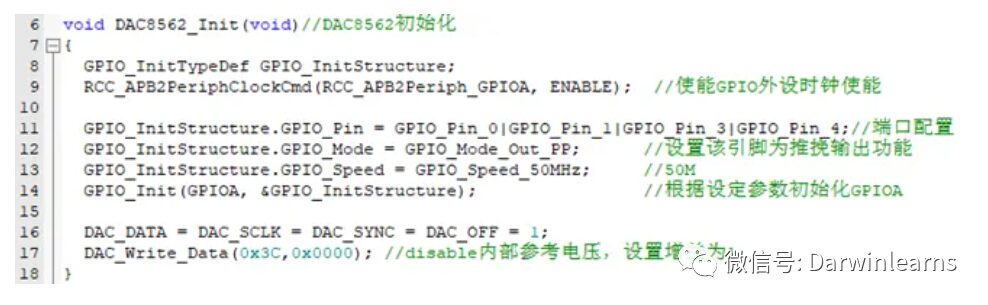
DAC8562 Initialization Configuration
✔ Temperature Detection and Heat Dissipation
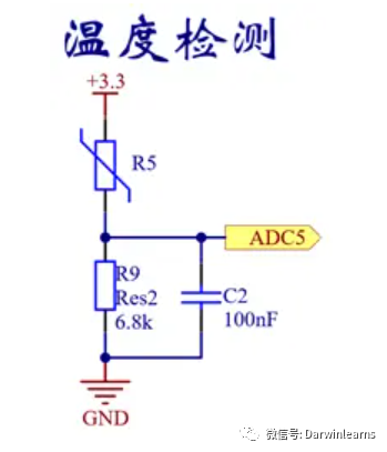
Temperature Detection Schematic
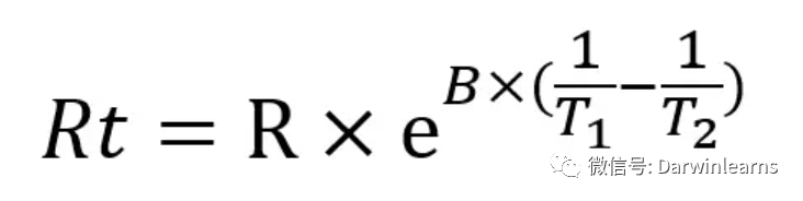
NTC Thermistor Resistance as a Function of Temperature
Here, T1 and T2 refer to the Kelvin temperature, Rt is the resistance of the thermistor at temperature T1, R is the nominal resistance of the thermistor at temperature T2, and B is the material constant of the thermistor.
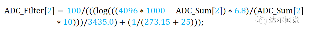
Temperature Calculation Program
ADC_Filter[2] is the calculated temperature result, in Kelvin; ADC_Sum[2] is the accumulation of 1000 samples from the 12-bit ADC.
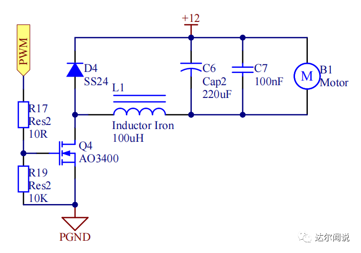
Heat Dissipation Fan Control Circuit Schematic
The heat dissipation fan control circuit is essentially a low-side Buck converter circuit. The microcontroller generates PWM to drive the field-effect transistor. By adjusting the PWM duty cycle, the voltage across the fan can be controlled, thus regulating the fan speed. The fan speed is determined by the temperature measured by the thermistor, achieving automatic on/off and automatic speed regulation based on temperature.
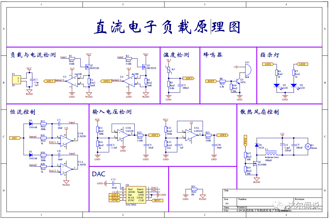
Complete Schematic of the Project
The schematic does not show the microcontroller-related circuits, only the key IO interfaces. Readers can freely develop based on their needs regarding microcontroller selection and other expansion functions.
Electronic Load Code Download:
Reply “STM32 Electronic Load” on WeChat for the download link.

<<< STM32 Project Collection >>>
<<< Raspberry Pi Project Collection >>>
<<< ESP32 Project Collection >>>
<<< ESP8266 Project Collection >>>
<<< Arduino Project Collection >>>
<<< Darwin Project Share Series >>>