
This project integrates off-grid inversion, MPPT for battery charging, and energy interaction switching with the grid. It is a machine that completes all application scenarios in solar off-grid power generation. Due to the integration of many functions, it may require some upgrades to finalize! Technical documentation will be updated step by step as the hardware is perfected, and shared with everyone!


Currently, many inverters do not have MPPT, and the switching between grid priority or inverter priority is not very mature. This is because there is no mature solution from the core control side, requiring multiple chips to work together. Therefore, to simplify the circuit, it is necessary to redesign a single-chip solution from the core control chip that can include the following functions:
1. Integrated MPPT charging, designed as a single-phase BUCK DC-DC method to enhance this efficiency, specifically tailored for the inverter integrated machine based on previous MPPT mature experiences.
2. Integrated photovoltaic charging current detection, using an external operational amplifier to send photovoltaic current to the CPU for MPPT calculations, simplifying the process.
3. Integrated H-bridge for inverter with 4 PWM outputs, using the most efficient and stable dual-edge modulation SPWM output, directly from the chip to 4 SPWM outputs, further simplifying the peripherals.
4. Integrated grid locking phase, using a unique hardware phase-locking method to handle interference and noise from the grid within the chip, ensuring strict symmetry between the inverter output AC voltage and the grid AC signal. When grid power is available, the inverter voltage follows the frequency and phase of the grid power, ensuring a smooth transition and no voltage difference during switching.
5. Integrated communication control function, allowing users to set inverter priority or grid priority, and output MPPT data, inverter data, and grid data in real-time to the outside, which is very useful for lithium battery systems that require such data for further control. With this, the foundation for remote control and monitoring is established, and some colleagues have started developing upper computer software that can provide monitoring once this is available.
6. Paired with specially developed current sensing components to simplify the short-circuit protection circuit, the unique chip internal short-circuit protection action circuit allows the inverter to execute constant current + current inner loop mode in the event of an external short circuit, avoiding damage to the IGBT and driver. Additionally, this mode will optimize load capacity, allowing a 3KW high-frequency machine to start a 2P air conditioner without any issues, with the inverter feeling virtually no pressure during startup.
7. Integrated 5 major protection functions: over-voltage, under-voltage, over-temperature, short-circuit, and overload.
8. This time, the STM32 chip is used to realize the above functions, with the preliminary model set as: STM32F103RET6. I used a separate mode of control board + power mainboard, utilizing a plug-in structure for easier debugging.
Basic Parameters
Rated input voltage of the inverter: 24V
Voltage range: DC21-DC30V
Output voltage: AC220V, pure sine wave output frequency: 50Hz, 60Hz (automatically follows the grid frequency and remembers)
Rated output power: 2000W
MPPT input voltage range: PV/30V-180V
MPPT charging current: 30A
Grid and inverter switching time: <10ms
Next, we will analyze the circuit step by step, starting from the mainboard…
Read the original article to download
-
Control board circuit diagram PDF file (see post 7, 2017-3-23)
-
Mainboard circuit diagram PDF file (see post 108, 2017-5-5)
Photos of the control board are as follows:
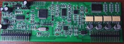
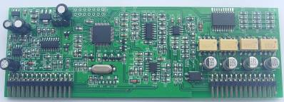
Analysis of the control board, small signal circuit part
01
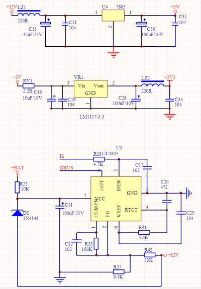
Auxiliary Power Control Part
Since the design is for a DC24V battery input, the CPU and other chips are powered by low voltage. Therefore, an auxiliary power supply is needed to step down the input DC24V to several suitable voltages for the chips and drive circuit power supply. Here, a classic UC3845 chip is used to create a flyback power supply, as shown in the figure. The transformer is not shown because it is on the mainboard, which will be visible when the mainboard circuit diagram is updated later. Here, only the small signal control part is analyzed. The auxiliary power supply generates 12V, 5V, and 3.3V voltages; the 12V voltage has an isolated group, which will be provided for the IGBT driving of the inverter. The 5V is provided for the operational amplifier, and the 3.3V is provided for the CPU. This concludes the auxiliary power supply part.
02
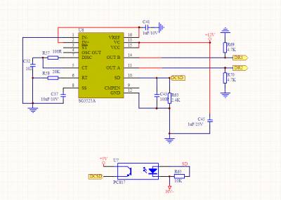
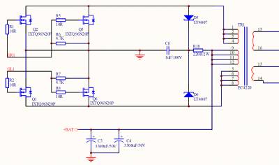
Inverter Boost DC-DC Part
To simplify the boost part, I still used the classic SG3525 chip to implement push-pull boosting, currently boosting DC24V to DC400V, which is the most suitable circuit type, and the driving is relatively simple.
The optocoupler at the bottom of this circuit is used to isolate feedback and directly control the SD pin of the SG3525. As long as the boost voltage exceeds DC400V, the optocoupler will conduct, raising the SD pin voltage and automatically reducing the PWM duty cycle. This achieves a form of voltage regulation, as precise regulation is not required here, the simpler the circuit, the better!
03
CPU Part
This time, the STM32F103RET6 is used for the main control part, which is a 64-pin chip, providing sufficient resources and IO to implement the functions of this board.
Due to the high speed of this chip, specific performance details can be searched online, so I won’t repeat them here. This allows for a significant simplification of many external components, especially making the hardware much cleaner. As follows:
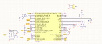
Let’s take a look at the signal definitions step by step.
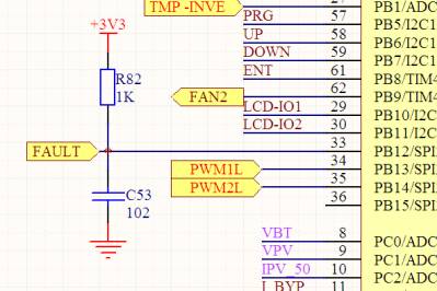
The following 4 PWM channels correspond to the inverter’s H-bridge, driving the upper and lower switches of the left and right arms, generating SPWM to achieve sine wave output.
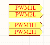
The following two groups of PWM are used to generate phase-interleaved 180-degree duty cycles for BUCK mode MPPT charging, with the duty cycle set from 0-96%.

This one is used for fault detection of the inverter SPWM current limiting, achieving short-circuit protection for the inverter and ensuring load capacity without blowing the transistors.
04
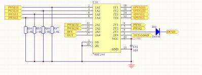
PWM Output Level Conversion Part
To isolate the PWM signal from the CPU to prevent noise interference from external drives, the PWM signal is buffered using a level buffer chip.
This allows the 3.3V PWM to be buffered through this chip, further enhancing noise resistance, which is beneficial for the subsequent input to the driver.
05
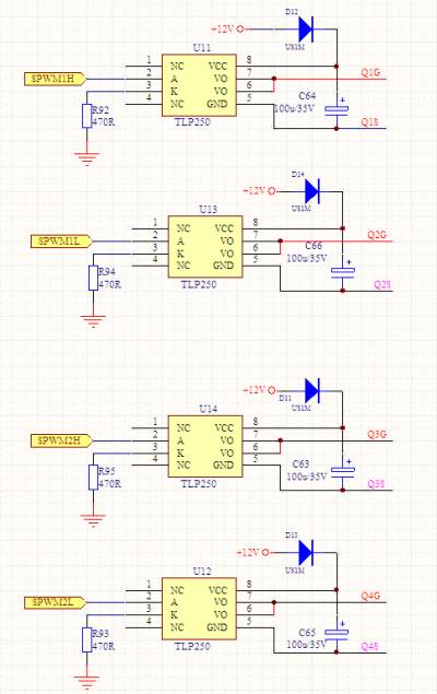
Optocoupler Driving Part
The design uses a TLP250 optocoupler driver, with secondary power supply adopting a bootstrap method to simplify the power supply side circuit.
06
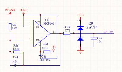
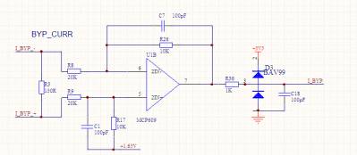
MPPT
MPPT requires current detection from the solar panels. An operational amplifier is used to amplify the voltage across the sampling resistor, with a gain of 51 times.
This allows the 3.3V PWM to be buffered through this chip, further enhancing noise resistance, which is beneficial for the subsequent input to the driver.
07
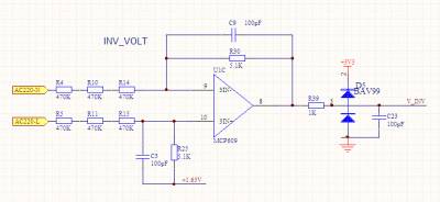
Grid Phase Lock
Grid phase locking and synchronization, VRMS detection first uses differential to reduce the grid voltage to 0-3.3V, within the detection range of the CPU’s ADC. Additionally, a comparator is used to generate a square wave synchronized with the grid frequency, entering the DSP for zero-crossing and grid cycle calculations. The program requires these parameters for phase locking and synchronization.
08
Inverter AC220V Voltage Detection
Using differential to attenuate the 220V voltage output from the inverter to a 0-3.3V corresponding signal, which is input to the CPU’s ADC port. The program uses this parameter to achieve AC220V voltage closed-loop and instantaneous value feedback.

09
Inverter Load Current Detection
The output signal from the transformer on the mainboard is sampled across a resistor to obtain a sine wave voltage, which is conditioned through an operational amplifier and sent to the CPU’s ADC for IRMS detection, enabling overload protection and power/current display.
10
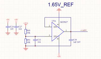
1.65V Reference Bias Voltage
The 1.65V reference bias voltage is generated by dividing the 3.3V voltage through two identical resistors, allowing the operational amplifier to follow through a stable bias of 1.65V. Due to the nature of AC parameters, this 1.65V is used for adding signals from various AC signals.

The above updates the mainboard circuit diagram. Next, we will look step by step at the components on the mainboard. The mainboard has a level DCDC push-pull boost, plus the inverter part and the MPPT charging part. First, let’s take a look at the DCDC push-pull part, as follows: a very classic push-pull circuit. Since the input of this circuit is 24V, using switching transistors rated for 80-100V is sufficient. The parameters in the figure are for IXTQ96N20, which can also be used for DC48V. In practice, using IRFB4310’s 100V transistor is sufficient. D5-D6 in the figure are used to absorb the spikes from the push-pull switching transistors, enhancing the safety of the transistors.
Questions from Readers
Dear author, I have a few questions:
1. Does the IGBT driver need negative voltage? Under what circumstances is negative voltage unnecessary?
2. Why not use a single boost for the DC-DC part? Wouldn’t that be simpler and more efficient?
3. Is the voltage sampling operational amplifier output pulled up with a diode to clamp the voltage at 3.3V to protect the chip’s IO port?
4. Will there be any delay in the bootstrap driving switch?
1. The IGBT driver does not necessarily need negative voltage. If the switching current is too large, due to Miller effect, it may cause misfiring of the upper and lower switches. Having negative voltage can minimize the possibility of misfiring.
2. The BOOST’s boost ratio cannot achieve such a high value, and the peak current through the transistors is very high, leading to low core utilization, which is why it was not used here.
3. Yes, that’s correct.
4. All drivers will have some delay, and all signal transmissions have delays, but this delay can be ignored in this case.

The text is limited to extract a portion of the content. For more exciting content, please click to read the original article!!!
Previous Highlights Review

-
【Li’s Lecture】 Key Points of Flyback Transformer Design (Part II)
【DIY Share】 100-150W Streetlight Power Supply Design (Supports Tri-Color Dimming)
Fourier_Laplace_Z Transform Study Notes
【DIY Share】 93+% High-Efficiency 12V 5A Adapter
Key Technology Deep Dive into Charging Pile Charging Module
Trying out LCC Topology, While Discussing Learning Methods