A Semiconductor Milestone for a 22-Year-Old: A DIY Chip Integrating 1200 Transistors.
About 30 miles from Bell Labs, a 22-year-old is chasing chip manufacturing giants in his garage.
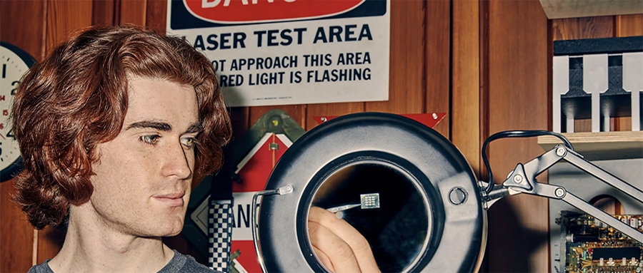
In the 1970s, chip manufacturing giant Intel developed the world’s first commercial microprocessor, the 4004. In August 2021, Sam Zeloof announced his own semiconductor milestone—the Z2 chip he created in his garage, which uses the same technology as the 4004 microprocessor.
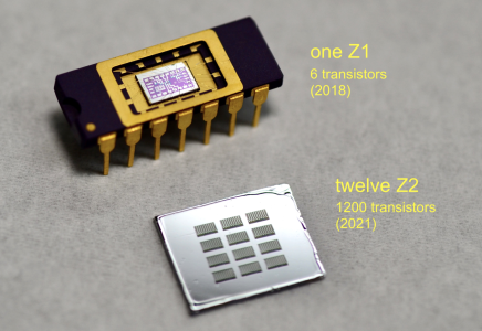
▲ Zeloof’s Z1 and Z2 Chips
Inspired by renowned hacker and hardware designer Jeri Ellsworth’s successful homemade transistors, Zeloof began exploring self-research in chip design.
In 2018, Zeloof created the first generation Z1 chip, which utilized 5-micron PMOS circuit technology and integrated 6 transistors. Just three years later, the second-generation Z2 chip was born, integrating 1200 transistors—200 times more than the first chip.
According to Moore’s Law, the number of transistors that can fit on an integrated circuit doubles every 18 to 24 months. From this perspective, Zeloof’s chip evolution speed can be said to far exceed Moore’s Law.
Although Zeloof’s chip technically lags behind Intel’s, he often jokingly claims that his progress is faster than the early advancements in the semiconductor industry.
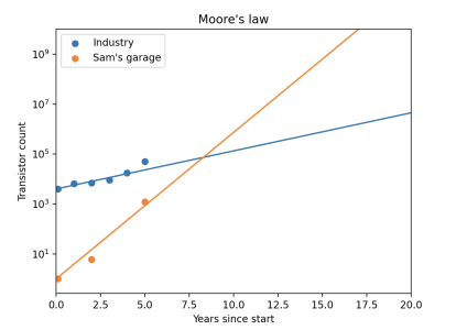
▲ Comparison of Commercial Chips Under Moore’s Law and Zeloof’s Self-Research Chips
From the birth of the transistor at Bell Labs in 1947 to its widespread implementation today, chip manufacturing technology has developed to 5nm, with chip giants like Intel dominating the market. It seems laborious and thankless to make a chip by oneself. So what inspired Zeloof to create his own chip, and how did he succeed in such a rudimentary environment? We found answers from his blog and YouTube channel.
Transforming from Transistors to Chips in 2 Years
In 2010, Ellsworth successfully manufactured thumb-sized transistors in her own lab. By coincidence, after seeing a video Ellsworth posted on YouTube, Zeloof, then a high school senior, began his exploration in 2016.
In addition to replicating Ellsworth’s transistor manufacturing project, Zeloof aimed to develop the world’s first homemade chip. Within just 2 years, he achieved this goal. The process from individual transistors to integrated circuits historically took about ten years. He stated, “Ellsworth pushed it forward significantly while reminding the world that these seemingly unattainable industries can start from more ordinary places, which is very valuable.”
In 2018, Zeloof’s first chip was born during a gym class, featuring 6 transistors and capable of process and equipment testing. He mentioned on his blog, “Making this chip required 66 steps and took about 12 hours.”
On the chip, Zeloof chose the dancing bear as a symbol, representing the American rock band Grateful Dead.
▲ The Dancing Bear on Zeloof’s Chip
In August 2021, building on the Z1 chip, Zeloof developed the Z2 chip, which contains 1200 transistors, each measuring just 10 microns, comparable to the size of a red blood cell.
The Z2 uses a polysilicon gate technology, unlike the Z1, and can operate at very low voltages, with a threshold voltage of only about 1 volt, meaning they can be packaged in simpler chips.
By the end of 2021, he began researching a temporary circuit design capable of performing simple addition, hoping to match the scale of Intel’s groundbreaking 1971 4004 chip, which had 2300 transistors.
Manufacturing in the Garage
Process Steps Similar to Wafer Fabrication
Chip manufacturing is often described as the most difficult and precise manufacturing process in the world. How did Zeloof accomplish such a complex process in his garage?
Chip manufacturing is characterized by photolithography, where the most important aspect is to layer different semiconductor materials on the silicon wafer according to the chip design layout, forming a structured layer of circuit components.
Zeloof first used a diamond scriber to cut a 200mm wafer into half-inch square pieces, officially starting the chip manufacturing process.
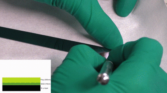
The first step is to coat the wafer with photoresist. Zeloof created a spin coater from recycled materials to evenly apply 100 microliters of photoresist on the half-inch square wafer. The spin coater spins at 4000 RPM for 30 seconds, evenly covering the wafer with photoresist, while excess photoresist is flung off. After that, it is dried on a hot plate at about 95 degrees Celsius for a minute, leaving a complete solid film.
▲ Spin Coater Applying Photoresist
The second step is exposure, where Zeloof’s homemade maskless lithography machine came into play. Compared to ASML’s large-area exposure contact lithography machines, maskless lithography is suitable for early-stage processes that are not very mature and require small batch production of samples. After generating images on a computer, the maskless lithography machine, DLP (Digital Light Processing) projector, and some optical devices can project the images down and reduce them to the size of the wafer.
After exposure, the next step is development. The wafer is placed in a potassium oxide solution for about a minute to etch away the exposed photoresist, followed by rinsing off the remaining developer with water.
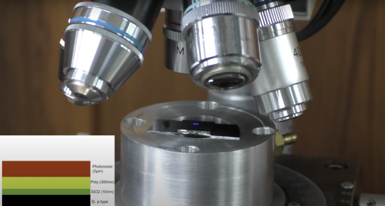
After development, Zeloof inspects the wafer’s components using an electron microscope. If issues arise, he repeats the experiment using different exposure or development times.
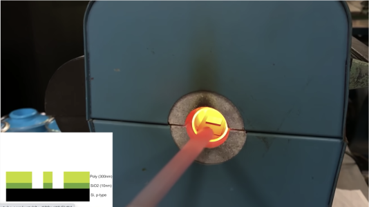
Then etching and stripping occur. After the image is formed in the photoresist, Zeloof uses etching agents to transfer it to the underlying polysilicon layer, and after etching, he strips the photoresist mask layer with acetone.
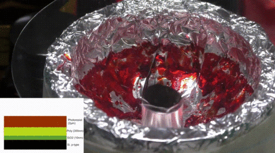
In the cleaning and drying step, he places the wafer in a phosphorus solution and bakes it at temperatures exceeding 1000 degrees Celsius for about 45 minutes, driving phosphorus atoms into the chip defined by lithography to adjust its conductivity.
▲ High-Temperature Baking Process
The chip is placed in a vacuum chamber to sputter or thermally evaporate metal, and then the entire process is repeated to encapsulate the metal layer. After completion, Zeloof places the entire wafer in a warm phosphoric acid solution to etch away the remaining aluminum, indicating that the chip has been successfully manufactured.
Finally, Zeloof thoroughly inspects the chip and takes numerous close-up photos to measure parameters such as gate length, width, and layer thickness.
In August 2021, Zeloof connected the Z2 to an old HP square beige semiconductor analyzer for testing. A series of smoothly rising current-voltage curves appeared on its glowing green screen, proving the success of his homemade chip. “This curve is amazing,” Zeloof said, “after spending all day soaking this little crystal fragment in a beaker of chemicals, this is the first sign of success.”
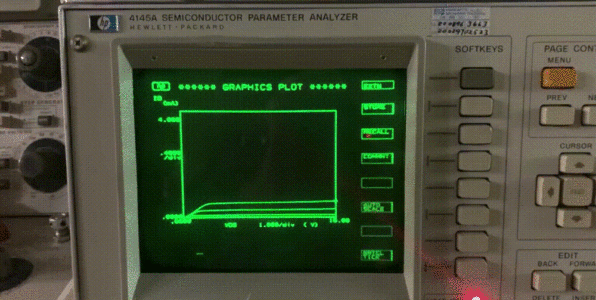
▲ Current-Voltage Characteristic Curve of Z2
Afterward, he shared all the manufacturing steps and explanations on his blog, Twitter, and YouTube, with these videos garnering millions of views. Meanwhile, seasoned professionals in the semiconductor industry provided him with practical tips.
Today’s commercial wafer fabs follow a process similar to the steps mentioned above, gradually adding and removing materials at different stages of chip design. However, the most advanced chip processes are completed by machines rather than manually, allowing billions of transistors to be tightly packed together. Zeloof’s success demonstrates that chips can indeed be made from sand in a garage.
Recycling Materials from Second-Hand Websites, Homemade Lithography Machine
So how did he solve the equipment shortages encountered during the chip manufacturing process?
The modern chip manufacturing process requires expensive HVAC (Heating, Ventilation, and Air Conditioning) systems to eliminate dust in the manufacturing plant, to avoid affecting the chip manufacturing machines worth billions of dollars. Given the limited resources and space, he couldn’t have similar equipment and technology.
Thus, he read patents and textbooks from the 1960s and 70s, learning how engineers from pioneering companies like Fairchild Semiconductor manufactured chips on ordinary workbenches. “They described methods using X-Acto blades, tape, and some beakers, instead of saying, ‘we have this $10 million machine the size of a room,’” Zeloof said.
In addition, there are many devices required in the chip manufacturing process, and Zeloof could only choose from eBay and other auction sites. He discovered inexpensive chip equipment from the 1970s and 80s. Many of these devices, due to years of neglect, required extensive repairs and maintenance, but repairing them was certainly easier than acquiring modern laboratory machines.
What surprised Zeloof the most was finding a broken electron microscope, which he could use to inspect the chips for defects. This microscope, which might have been worth $250,000 in the early 90s, he bought and repaired for just $1,000.
In the chip manufacturing process, Zeloof still lacked many devices and technologies, and sometimes he had to improvise. The lithography machine, an essential device in chip manufacturing, transfers early microscopic design details onto the chip and is crucial for subsequent processing steps. He organized a conference projector purchased from Amazon and an electron microscope into a makeshift “garage lithography machine,” which can project image designs at a small scale onto silicon wafers.
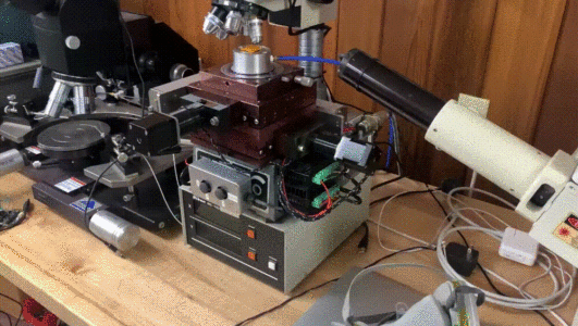
▲ Zeloof’s Homemade Lithography Machine
This lithography machine has recently been updated by Zeloof, capable of printing details as small as about 0.3 microns or 300 nanometers, which is already comparable to the commercial chip technology of the mid-90s. Now, he is considering building related functions in chips the size of Intel’s 4004. “I want to further push homemade chips and let people believe that we can do these things at home,” he said.
Zeloof will graduate from Carnegie Mellon University this spring and has been contemplating the position of DIY chip manufacturing in the modern technology ecosystem.
From an industry perspective, today’s technology and equipment have facilitated DIY experiments, including easily accessible robotic equipment and 3D printers, as well as mature hardware development platforms like Arduino microcontrollers and Raspberry Pi. “But these chips are still produced in some large factory, which has minimal effect on the ease of chip manufacturing,” Zeloof said.
Initially, when this 22-year-old began introducing his project goals on his blog, some industry experts emailed him saying it was impossible. However, Zeloof believes that the abundance of tools in this industry makes small-scale chip manufacturing possible.
Zeloof’s family has supported him while also providing some help. Mark Rothman, a semiconductor engineer with 40 years of experience in chip engineering and a friend of Zeloof’s father, provided Zeloof with some safety advice but thought the idea of making chips in a garage was fanciful.
After witnessing Zeloof’s success, this semiconductor engineer gradually changed his perspective and said, “He did something I never thought people would do.”
Conclusion: Small Workshops vs. Large Factories
Zeloof is developing his third “garage chip,” the Z3, which will further explore the manufacturing of complete microprocessors. This chip, born in a garage, may not be installed in your phone, computer, or game console, but it showcases more possibilities for “inventors” without million-dollar budgets.
Currently, chip manufacturing technology often requires investments of millions or even billions of dollars, and such a high entry barrier increasingly monopolizes chip manufacturing technology in the hands of large companies. Only by returning technology to society can we foster innovation and development.
Although small-scale chip workshops may not solve the broader chip supply shortage, in the future, as small-scale chip manufacturing plants increase, they may promote rapid advancements in semiconductor technology.
Source: Chip Things