Click the “Public Account” above to subscribe!
Samsung has finally emerged from the explosion scandal, driven by rising prices of DRAM and NAND, pushing Intel off its semiconductor throne after 14 years. The glory is indeed unparalleled. Although the market is expected to correct in the second half of the year, overall DRAM is still expected to grow by 39% compared to last year, while NAND is expected to grow by 25%. These two have helped Intel reach its peak, truly a case of success and failure intertwined. Speaking of NAND Flash, it and its brother NOR Flash are among the most important inventions of the 20th century. Their birth and development have been quite tortuous, born in Japan, raised in the United States, and now shining brightly in South Korea. Today’s historical story begins with its inventor, Fujio Masuoka, and his dramatic employer.
History
Intel invented EPROM early on, which is a type of memory that can be erased with ultraviolet light. Compared to ROM, its contents can be updated and can last for 10 to 20 years; old computers’ BIOS were stored in this.
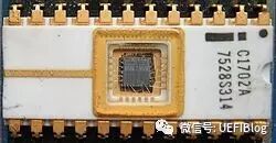
(Intel 1702)
Its top must be covered to prevent it from being erased by ultraviolet light in sunlight. Later, Intel invented an upgraded version called EEPROM in 1978, which can be erased electrically without the need for sunlight, making it much more convenient, but the read and erase speeds were very slow.
At this time, our protagonist Fujio Masuoka entered the scene. He joined Toshiba in 1971. Inspired by EEPROM, he began to study a type of EEPROM that could be erased quickly during his nights and weekends. In 1980, he made a breakthrough and applied for a patent for something called simultaneously erasable EEPROM. However, the seniority system of large Japanese companies buried this groundbreaking invention for four years.
“I was finally promoted and could go to the factory without approval to have workers help make samples,” Masuoka said. When he brought his samples to that year’s IEEE conference, NOR Flash caused a sensation, so much so that when he returned to Japan, his boss was constantly harassed by calls from Intel wanting samples. He was rewarded with a few part-time helpers. Meanwhile, across the ocean, Intel, upon receiving the samples, immediately dispatched over 300 engineers to develop their version. Due to the rapid erase speed of this newly invented EEPROM, Masuoka’s colleagues suggested naming this technology Flash, echoing the quick flash of a camera’s flash.
Toshiba did not treat NOR Flash technology as a treasure; they simply did not want others to interfere, so they continuously sued any company that hoped to get involved, such as TI. However, Masuoka did not stop his pursuit and invented NAND Flash in 1986, significantly reducing manufacturing costs. For his contributions, Toshiba rewarded him with a few hundred dollars and a high but leisurely position. As an engineer, he could not tolerate such treatment and had to resign to continue research at the university.
Toshiba’s shortsightedness soon brought market punishment. The Flash market rapidly expanded, reaching hundreds of billions of dollars by the late 1990s, with Intel being the market leader while Toshiba held a very small share (almost none for NAND and NOR). For a long time, Toshiba even denied that NOR Flash was invented by him, claiming it was invented by Intel. It wasn’t until IEEE awarded Masuoka a special contribution award in 1997 that they changed their tune.
Masuoka felt that his contributions were erased by Toshiba, and in 2006 he angrily sued the company, demanding 1 billion yen in compensation. In the end, he reached a settlement with Toshiba, receiving 87 million yen (approximately $758,000). Masuoka did not stop his steps; after obtaining over 200 patents, he is still pursuing the next big thing.
Undoubtedly, Masuoka is a hero. Some say he should be awarded the Nobel Prize; he is one of the few inventors I can still remember, while many other technical inventors have faded into obscurity. This story also reflects the bureaucratic nature and ailments of large Japanese companies.
NOR VS NAND

So what are NOR Flash and NAND Flash? Let’s first take a look at what their chips look like:
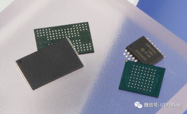
(Left is NAND, right is NOR)
I won’t discuss their electrical principles, as there aren’t many interested in that. Here, we mainly focus on their commonalities and characteristics.
1
Commonalities
A. Both are non-volatile storage media. That is, they do not lose content when power is lost.
B. Both require erasure before writing. In fact, a bit in NOR Flash can change from 1 to 0, but to change from 0 to 1, the entire block must be erased. NAND Flash also requires erasure.
2
Characteristics
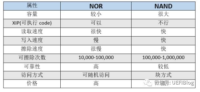
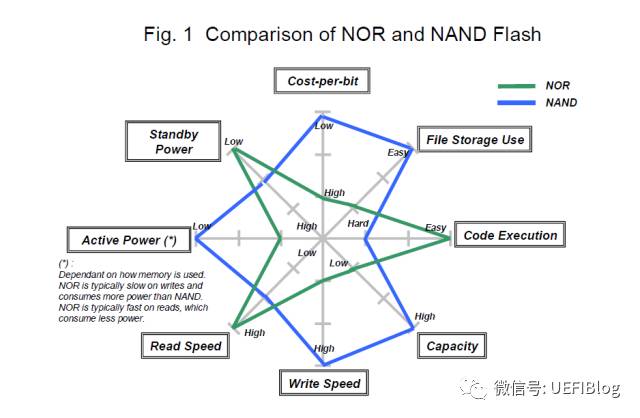
Characteristics determine which type of Flash to use, and I have summarized a table:
If we compare Micron’s own NAND and NOR, the detailed speed data is as follows:
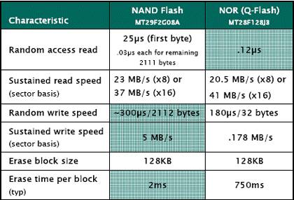
(Data source: Micron)
If we look at random read speeds alone:
(Data source: Micron)
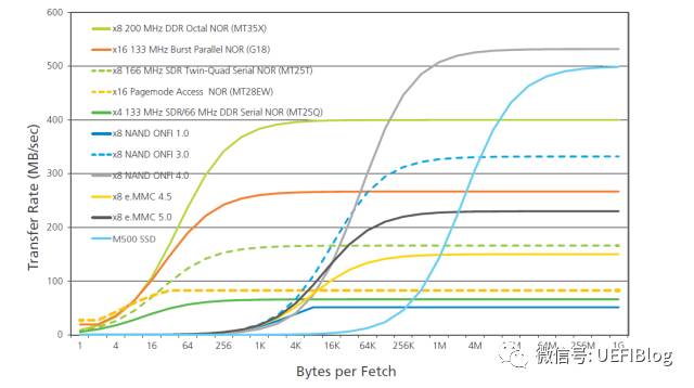
If we use the popular relationship diagram now, it looks like this:
(Data source: Toshiba)
Application Scenarios
NOR and NAND Flash can be found in both PCs and mobile phones.
1
NOR Flash
NOR Flash is somewhat similar to ordinary memory in that it supports random access, which also gives it the feature of supporting XIP (eXecute In Place), allowing it to execute programs like ordinary ROM. This makes it an excellent carrier for code that needs to be executed at boot, such as BIOS.
NOR Flash can be divided into Parallel NOR Flash and Serial NOR Flash based on the different interfaces with the host.

Parallel NOR Flash can connect to the host’s controller, and the stored content can be directly mapped to the CPU address space, allowing the CPU to access it without copying it to RAM. NOR Flash was initially used in BIOS with this interface, called FWH (Firmware HUB). However, due to its parallel interface, it is slow and has now been largely phased out. Serial NOR Flash is cheaper than Parallel NOR Flash and connects to the host, which is the PCH, mainly through the SPI interface.
Currently, almost all BIOS and some set-top boxes use NOR Flash, with sizes typically ranging from 1MB to 32MB, and it is expensive.
2
NAND Flash
NAND Flash is widely used in various storage cards, USB drives, SSDs, eMMC, and other large-capacity devices. Its chips can be classified into SLC (Single-Level Cell), MLC (Multi-Level Cell), and TLC (Triple-Level Cell) based on the number of bits stored in each memory cell. Among them, SLC can store 1 bit, MLC can store 2 bits, and TLC can store 3 bits in a single memory cell.
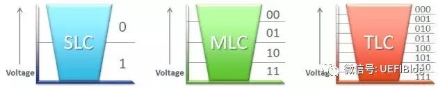
The more bits stored in a single NAND Flash memory cell, the worse the read and write performance and the shorter the lifespan, but the cost is lower.
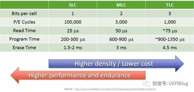
High-end SSDs typically choose MLC or even SLC, while low-end SSDs choose TLC. SD cards generally select TLC.
3
Others
1. In the earliest mobile phones and other devices, both NOR Flash and NAND Flash were present. NOR Flash was small and supported XIP, so it was responsible for initializing the system and providing the driver for NAND Flash, similar to a Bootloader. NAND Flash stored data and OS images. Samsung was the first to propose the concept of Norless, embedding the NAND Flash driver in its CPU on-die ROM, copying a small segment of NAND Flash to the lower end of memory as a bootloader, thus saving the expensive NOR Flash, reducing the cost and complexity of the phone’s motherboard. Gradually, NOR Flash has slowly disappeared from mobile phones.
2. The biggest problem with NOR Flash is its slow erase/write speed and limited rewrite cycles, but this rarely causes a decrease in BIOS speed or damage. Do you know why?
Conclusion
NAND Flash is more likely to experience bit flips compared to NOR Flash, so error detection/correction (EDC/ECC) algorithms must be employed. Additionally, NAND Flash gradually develops bad blocks with use; we often use the FAT file system on NAND Flash SD cards. If everyone has gone through the previous articles (link), they will know that the file allocation table is frequently rewritten, and the number of erase cycles for each block is a decisive factor in NAND Flash’s lifespan. How can we balance the erase cycles of each block and find replacements for potential bad blocks? Typically, a special software layer is needed to implement bad block management, wear leveling, ECC, garbage collection, etc. This software layer is called FTL (Flash Translation Layer). Depending on the location of the FTL, Flash Memory can be divided into Raw Flash and Managed Flash:
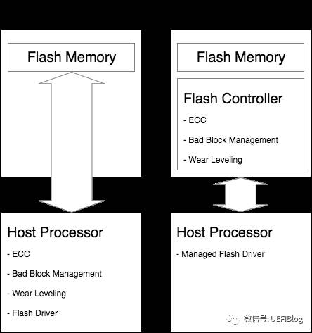
Initially, everyone used raw Flash, with the FTL implemented entirely by the driver. Later, with the development of SD and eMMC, the device firmware implemented the abstraction.
The principle of FTL will be the main content of our next article.