The camera of the Xiaomi 11 Pro/Ultra smartphone uses the CIS (CMOS Image Sensor) model Samsung ISOCELL GN2 (hereinafter referred to as GN2). The strength of this CIS lies not in the pixel count, but in its overall size of 1/1.12 inches.
Although this phone was released some time ago, the GN2 may still be the largest CIS currently used in smartphones, larger than those used in the Huawei Mate40 Pro/P50 series (the former uses Sony IMX700, while the latter may use Omnivision OV50A) and the recently popular Vivo X70 Pro camera main sensor (Sony IMX766V). The Sony IMX766 is also a popular 50MP CIS in smartphones today; while 1/1.56 inches can also be considered a “large sensor,” it still does not compare to the Samsung GN2.
Two years ago, when we first discussed the 100MP camera in Xiaomi phones, we were still amazed by the size of 1/1.33 inches, and now just a blink of an eye later, it has become 1/1.12 inches. In fact, this size of 1/1.12 inches is already larger than the photographic monster Nokia 808 Pureview from nine years ago, which had a CIS size of 1/1.2 inches—at that time, it left many smartphone enthusiasts in awe.
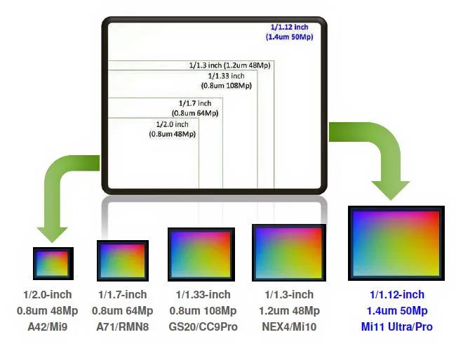
When digital compact cameras were still active, the CIS size of many high-end digital compacts was only about 1/1.7 inches. The contemporary Sony RX100 series has a CIS of just 1 inch—of course, this is just a comparison of image sensor sizes; moreover, a 1/1.12 inch CIS cannot be compared to mainstream mirrorless or DSLR cameras.
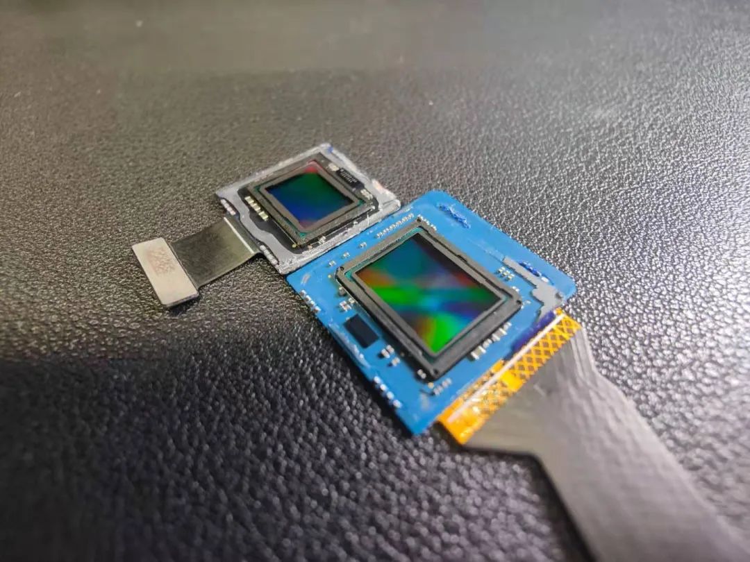
The image above is difficult to trace back to its original source (it may have originated on Twitter or Weibo); it mainly shows the size comparison between Sony IMX689 and Samsung GN2. However, the perspective effect presented by the shooting angle and focal length makes the GN2 appear larger. The Sony IMX689 is a CIS used in the OPPO Find X2 Pro phone last year, with a size of 1/1.4 inches—when OPPO launched this phone at the beginning of the year, there were many articles discussing how “a larger sensor can outperform smaller ones.” However, clearly, the IMX689 still pales in comparison to the GN2.
At the previous Hot Chips 33 conference, Samsung specifically discussed this 50MP GN2 image sensor. The Electronic Engineering Journal selectively provided some interpretations of it. Although it is unfortunate that this does not encompass the entirety of Samsung’s presentation, combining it with some of the information we have allows us to see the development path of smartphone camera CIS. Samsung’s developmental philosophy differs significantly from Sony’s, which we recently explored in our discussion of the development path of smartphone camera CIS from Sony’s perspective. Therefore, understanding the characteristics of the GN2 also helps us to discern another potential technological development path for CIS.
Another Direction for Single Pixel Size
Two years ago, when summarizing the development of smartphone camera CIS, we mentioned that the overall trend is that the size of individual pixels in CIS is becoming smaller. For example, around 2008, the pixel size of mobile CIS was generally around 1.4μm, which dropped to 1.12μm in 2011 and reached 0.9μm in 2018; the well-known 48MP CIS from 2019 had a single pixel size of 0.8μm; today, the single pixel size of 100MP CIS has reached 0.7μm.
Previously, Samsung LSI’s disclosed CIS roadmap indicated that the pixel size could shrink to 0.56μm/0.64μm in the 2021-2022 planning. At this year’s ISSCC 2021, Samsung publicly shared a paper on its 0.64μm pixels. Mid-year, Samsung announced the mass production of its first 0.64μm pixel sensor, specifically a 1/2.76 inch 50MP JN1; in addition, in September this year, Samsung launched the ISOCELL HP1—this 200MP image sensor also uses 0.64μm pixel sizes. Interested readers can check out the Samsung 0.64μm pixel PPT materials.
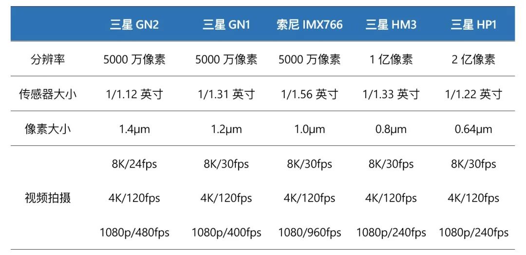
The star of this article, the Samsung GN2, has a single pixel size of 1.4μm—which is relatively large compared to mainstream smartphones. However, compared to the larger pixel (rather than higher pixel count) of the iPhone 13 Pro’s main camera, it is still slightly smaller. The single pixel size of the iPhone 13 Pro’s main camera CIS is 1.9μm. Of course, the Samsung GN2 has an advantage in pixel count, with a resolution of 8160×6144 totaling 50MP. Moreover, in terms of the entire area of the CIS, the GN2 is still the absolute largest.
In terms of smartphone camera CIS, it seems that Samsung is not merely pursuing smaller pixels, as smaller pixels typically face issues with sensitivity and dynamic range—solving these problems requires significant technical effort. Last year’s GN1 did not resort to stacking up to over a hundred million pixels. Sony’s promotion of the IMX766 also follows this line of thinking, indicating that simply producing smaller pixels will not become an overall trend for smartphone camera CIS in the short term.
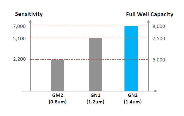
Samsung mentioned at Hot Chips that the 1.4μm single pixel size of GN2 brings a 33% increase in full well capacity, which means the maximum number of electrons that can be stored in the pixel well has increased, naturally leading to a greater dynamic range. In terms of photos, this translates to less noise—although I personally believe that within the scale of such a small imaging system like smartphone cameras, the difference may not be that significant.
For low-light environments, the GN2 can also utilize the previously known pixel binning technology, treating every four pixels as one to achieve a large pixel size of 2.8μm in dark conditions, enhancing its sensitivity. This is a relatively common method, sacrificing resolution to improve sensitivity, and Sony also employs this approach.
Additionally, in terms of pixel count, Samsung also provides the option for 100MP shooting with the GN2. Samsung’s official press release states, “In 100MP mode, the GN2 will use an intelligent re-mosaic algorithm to rearrange color pixels, targeting green, red, and blue, constructing three independent layers of 50MP frames. These frames are then up-scaled and merged to generate a 100MP photo.”
This statement is still somewhat vague; from the description, it seems to be some form of interpolation algorithm. After all, the physical pixel count of the GN2 is only 50MP, but this interpolation algorithm might be more advanced.
Besides the pixel layers, it is also worth mentioning that the GN2 adopts a dual-layer die stacking. One layer is the pixel layer: where the 50MP pixels reside. The other die contains the ADC (Analog-to-Digital Converter) and image processing digital circuits—this layer uses a 28nm process. This stacking solution is not new; we have previously introduced Sony’s CIS stacking technology in another article.
A Unique Technique: Staggered HDR
How to achieve HDR (High Dynamic Range) seems to be an eternal theme in contemporary smartphone photography. The marketing slogans of smartphone manufacturers, such as “clear even in backlight” and “illuminating your beauty at night,” are largely based on HDR: when shooting scenes with significant lighting contrast (like backlighting), HDR needs to play its role; both bright and dark areas must be considered within the same frame.
A common implementation of HDR is to take multiple photos with different exposure parameters after the user presses the shutter button once, and then stack and merge these photos. This way, details in both bright and dark areas of the scene can be preserved.
However, this approach has a side effect: since the multiple photos are taken at different time points, if the merging algorithm is not adequate when capturing moving subjects, it can result in blurriness or artifacts. To reduce artifacts caused by stacking multiple photos, one method should be to minimize the time interval between taking these photos.
When launching the GN2, Samsung announced a staggered HDR technology; this is not an interlaced single-frame HDR solution. Samsung mentioned that this technology relies on the rolling shutter characteristics. In the cover story of the May issue of Electronic Engineering Magazine, we specifically discussed the trend of CIS manufacturers implementing global shutter technology.
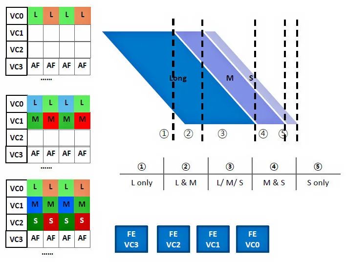
Samsung’s staggered HDR reportedly achieves HDR by using three different exposure methods within the time it takes to take a single photo. The specific method is illustrated in the above image. Based on rolling shutter, it first performs a long exposure, followed by a medium-length exposure, and finally a short exposure—each corresponding to dark, medium, and bright scenes, respectively, and then outputs and composes the results.
After the long exposure, the sensor immediately begins row output—from pixel rows to ADC. Before all pixel rows from the long exposure are completely output, the sensor will begin the medium-length exposure. This exposure phase actually begins outputting before all pixels from the long exposure are completely output. The short exposure process follows the same logic. Finally, the image processing unit of the GN2 will merge the photos to generate an HDR photo.
During this process, the sensor uses virtual MIPI channels to output the three exposure processes. The sensor performs long exposure on the dark areas and begins output via the VC0 virtual MIPI channel; subsequently, it corresponds to VC1 and VC2 virtual channels. Additionally, there is a VC3 virtual channel used to simultaneously send autofocus information generated by PDAF.
Unique PDAF Dual-Pixel Focusing
The PDAF (Phase Detection Autofocus) of the main CIS sensor has also been a hot technology in smartphone CIS over the past two years. Conventional dual-pixel autofocus divides a pixel into two parts. Each pixel contains two photodiodes used for imaging and focusing. When the phase alignment of the dual-pixel image is detected, it is considered to be in focus.
Previously, in the article The Development History of iPhone Cameras, we discussed how the iPhone represents a significant evolution in smartphone photography, with the PDAF technology having a corresponding evolution history on it. Up until the iPhone 11, the CIS achieved 100% coverage of PDAF focusing pixels.
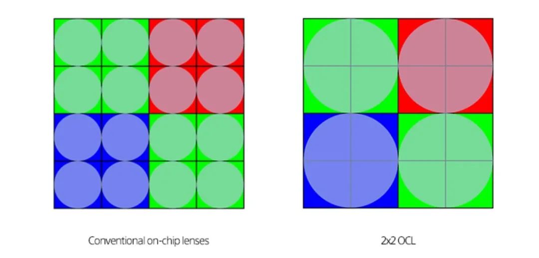
It is worth mentioning that Sony promoted its 2×2 OCL focusing technology last year—previously, we also introduced this. Essentially, it covers one microlens over every four pixels, allowing all pixels to participate in phase detection. Sony mentioned in their paper that this scheme can perform phase detection not only in vertical and horizontal directions but also diagonally, achieving cross-focus or diamond focus across the CIS coverage.
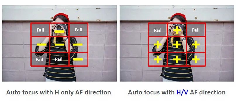
Generally speaking, if the two photodiodes of the phase detection pixel are merely arranged side by side, they will not be able to detect the phase difference of horizontal lines in the scene—or in other words, focusing on objects that contain horizontal lines will be problematic. Sony’s 2×2 OCL focusing scheme proves to be more applicable across various scenes.
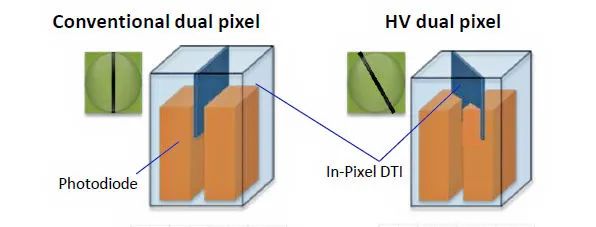
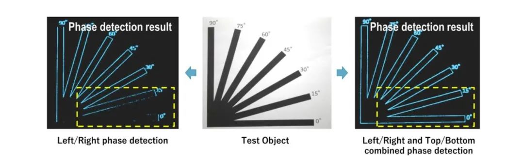
Samsung’s solution is to split pixels diagonally rather than vertically in half. The image above is a simple demonstration of the photodiodes of the GN2 phase detection pixels. The traditional method uses DTI (Deep Trench Isolation) to divide the phase detection pixels in half vertically. In contrast, the GN2 employs a diagonal DTI structure, allowing for high-efficiency focusing on both horizontal and vertical lines.
The image below illustrates the differences in focus capabilities between the two approaches. Clearly, a scheme that purely isolates phase detection subpixels vertically cannot detect phase differences in many areas—arranging the left and right pixels makes it almost impossible to detect phase differences in horizontal lines within the scene. On the other hand, the diagonal isolation method allows for more focusing scenarios, making it capable of cross-focus.
Of course, we do not know whether the implementation details and manufacturing processes pose additional challenges. Samsung noted that each pixel for PDAF uses two photodiodes, meaning that 100 million phase detection subjects are involved. The structure is designed to “not only vertically split pixels but also diagonally split pixels.” How this is achieved in terms of process and pixel structure is also worth studying. Additionally, improvements have been made for focusing in low-light environments and tracking moving objects.
ISO Dual Gain and Low Power Consumption Implementation
Regarding the issue of ISO dual gain, we have already introduced it in previous articles. The first smartphone to promote ISO dual gain in China should be the OPPO Find X2, which used the Sony IMX689. However, to this day, we still do not have a clear understanding of how smartphone camera CIS achieves dual gain.
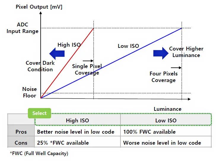
The Samsung GN2 has a separate dual gain control switch for every four pixels, allowing for two levels of ISO sensitivity to be adjusted. For brighter scenes, the sensor allows the pixel image signal to reach the full input range of the ADC, which is the low ISO mode; for dark scenes, it switches to high ISO mode, increasing pixel gain.
This type of scheme selects two native ISOs for different lighting scenarios, which Samsung calls Smart ISO Pro. “Using the iDCG (intra-scene dual conversion gain) solution, high and low ISO readings are obtained to achieve high dynamic range images, less affected by dynamic artifacts.” This also seems to be part of HDR; it is unclear whether this combines with the staggered HDR mentioned earlier.
“Additionally, in low-light environments, Smart ISO Pro can quickly capture and process multiple frames at high ISO, enhancing sensitivity to nearly 1,000,000 ISO, pushing nighttime imaging on smartphones to new heights.” This seems to be a somewhat exaggerated expression, and the common operation of multi-frame stacking in current smartphone night modes should be the same concept. As for ISO 1,000,000, this reflects the common operation of making nighttime shots look like daytime in many current smartphone night modes…
Another noteworthy point about the GN2 that Samsung has mentioned is its low power consumption. For the GN2 CIS, Samsung reduced the ADC supply voltage from 2.8V to 2.2V, achieving a 20% power reduction (311mW -> 244mW).
However, reducing the supply voltage also lowers the ADC’s input range, preventing it from receiving the full range of pixel voltages. To address this issue, Samsung added a -0.6V substrate feedback bias to the pixel die to level shift the output range; simultaneously, the ADC circuit on the logic die (the 28nm die) was optimized using a so-called low-threshold voltage transistor. The combination of both ensures a complete exposure range while reducing operational power.
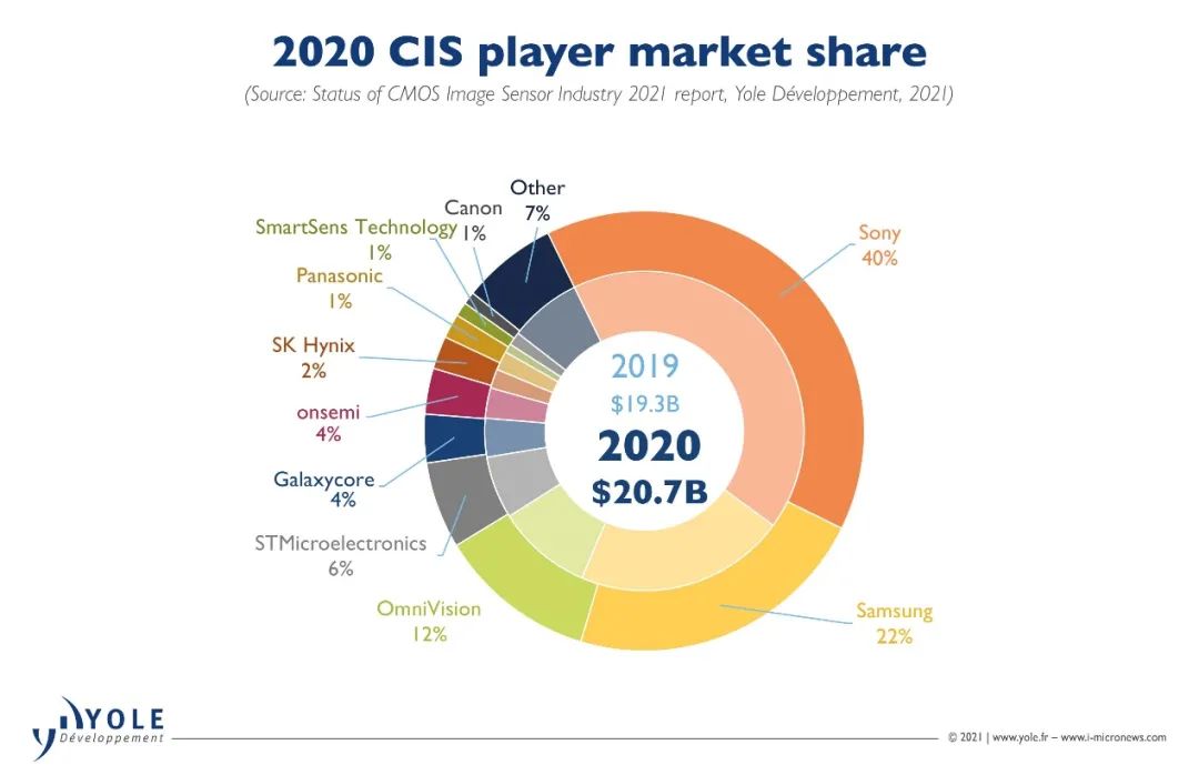
According to data released by Yole Developpement on the CIS market in 2020, Sony remains the absolute leader, accounting for 40% of the entire market. However, Samsung has somewhat narrowed the gap with Sony—though the extent is still relatively small, increasing from 21% two years ago to 22% in 2020; Sony has dropped by 2 percentage points.
The technological competition between the two companies has been quite intense over the past two years. Previously, Yole Developpement even wrote a report focusing on Samsung’s smartphone module comparison, emphasizing its innovation. The technological development of CIS can certainly be seen as a cornerstone of progress in smartphone photography, as evident from the marketing of smartphone manufacturers over the past two years.
Editor: Luffy Liu